- 您現(xiàn)在的位置:買賣IC網(wǎng) > PDF目錄373923 > AD7885 (Analog Devices, Inc.) LC2MOS 16-Bit, High Speed Sampling ADCs PDF資料下載
參數(shù)資料
| 型號(hào): | AD7885 |
| 廠商: | Analog Devices, Inc. |
| 英文描述: | LC2MOS 16-Bit, High Speed Sampling ADCs |
| 中文描述: | LC2MOS 16位,高速采樣ADC |
| 文件頁數(shù): | 10/16頁 |
| 文件大小: | 319K |
| 代理商: | AD7885 |
AD7884/AD7885
REV. C
–10–
Decoupling and Grounding
T he AD7884 and AD7885A have one AV
DD
pin and two V
DD
pins. T hey also have one AV
SS
pin and three V
SS
pins. T he
AD7885 has one AV
DD
pin, one V
DD
pin, one AV
SS
pin and one
V
SS
pin. Figure 6 shows how a common +5 V supply should be
used for the positive supply pins and a common –5 V supply for
the negative supply pins.
For decoupling purposes, the critical pins on both devices are
the AV
DD
and AV
SS
pins. Each of these should be decoupled to
system AGND with 10
μ
F tantalum and 0.1
μ
F ceramic capaci-
tors right at the pins. With the V
DD
and V
SS
pins, it is sufficient
to decouple each of these with ceramic 1
μ
F capacitors.
AGNDS, AGNDF are the ground return points for the on-chip
9-bit ADC. T hey should be driven by a buffer amplifier as
shown in Figure 6. If they are tied directly together and then
to ground, there will he a marginal degradation in linearity
performance.
T he GND pin is the analog ground return for the on-chip linear
circuitry. It should he connected to system analog ground.
T he DGND pin is the ground return for the on-chip digital
circuitry. It should be connected to the ground terminal of the
V
DD
and V
SS
supplies. If a common analog supply is used for
AV
DD
and V
DD
then DGND should be connected to the com-
mon ground point.
Power Supply Sequencing
AV
DD
and V
DD
are connected to a common substrate and there
is typically 17
resistance between them. If they are powered
by separate +5 V supplies, then these should come up simulta-
neously. Otherwise, the one that comes up first will have to
drive +5 V into a 17
load for a short period of time. However,
the standard short-circuit protection on regulators like the 7800
series will ensure that there is no possibility of damage to the
driving device.
AV
SS
should always come up either before or at the same time
as V
SS
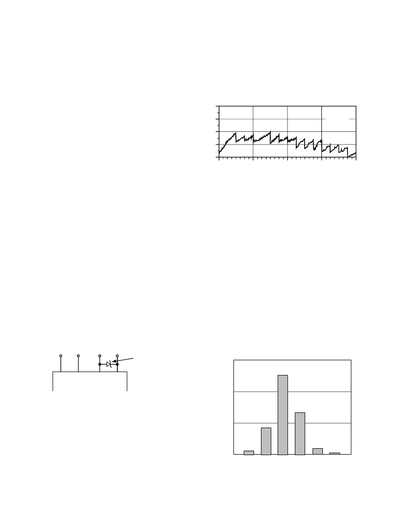
. If this cannot be guaranteed, Schottky diodes should be
used to ensure that V
SS
never exceeds AV
SS
by more than 0.3 V.
Arranging the power supplies as in Figure 6 and using the recom-
mended decoupling ensures that there are no power supply
sequencing issues as well as giving the specified noise performance.
AV
DD
V
DD
AV
SS
V
SS
+5V
+5V
–5V
–5V
AD7884/AD7885
HP5082-2810
OR
EQUIVALENT
Figure 12. Schottky Diodes Used to Protect Against
Incorrect Power Supply Sequencing
AD7884/AD7885 PE RFORMANCE
Linearity
T he linearity of the AD7884/AD7885 is determined by the
on-chip 16-bit D/A converter. T his is a segmented DAC which
is laser trimmed for 16-bit DNL performance to ensure that
there are no missing codes in the ADC transfer function. Figure
13 shows a typical INL plot for the AD7884/AD7885.
0
16384
32768
49152
65535
0
0.5
1.0
1.5
2.0
OUTPUT CODE
L
V = +5V
V = –5V
T = +25
°
C
Figure 13. AD7884/AD7885 Typical Linearity Performance
Noise
In an A/D converter, noise exhibits itself as code uncertainty in
dc applications and as the noise floor (in an FFT , for example)
in ac applications.
In a sampling A/D converter like the AD7884/AD7885, all in-
formation about the analog input appears in the baseband from
dc to 1/2 the sampling frequency. An antialiasing filter will re-
move unwanted signals above f
S
/2 in the input signal but the
converter wideband noise will alias into the baseband. In the
AD7884/AD7885, this noise is made up of sample-and-hold
noise and A/D converter noise. T he sample-and-hold section
contributes 51
μ
V rms and the ADC section contributes 59
μ
V
rms. T hese add up to a total rms noise of 78
μ
V. T his is the
in-
put referred noise in the
±
3 V analog input range. When operat-
ing in the
±
5 V input range, the input gain is reduced to –0.6.
T his means that the input referred noise is now increased by a
factor of 1.66 to 120
μ
V rms.
Figure 14 shows a histogram plot for 5000 conversions of a dc
input using the AD7884/AD7885 in the
±
5 V input range. T he
analog input was set as close as possible to the center of a code
transition. All codes other than the center code are due to the
ADC noise. In this case, the spread is six codes.
3000
0
2000
1000
C
(X – 2) (X – 1)
(X)
CODE
(X + 1) (X + 2) (X + 3)
Figure 14. Histogram of 5000 Conversions of a DC Input
相關(guān)PDF資料 |
PDF描述 |
|---|---|
| AD7885AAP | LC2MOS 16-Bit, High Speed Sampling ADCs |
| AD7885ABP | LC2MOS 16-Bit, High Speed Sampling ADCs |
| AD7885AN | LC2MOS 16-Bit, High Speed Sampling ADCs |
| AD7885BN | LC2MOS 16-Bit, High Speed Sampling ADCs |
| AD7886JP | LC2MOS 12-Bit, 750 kHz/1 MHz, Sampling ADC |
相關(guān)代理商/技術(shù)參數(shù) |
參數(shù)描述 |
|---|---|
| AD7885AAP | 制造商:Analog Devices 功能描述:16-Bit, High Speed Sampling ADCs |
| ad7885aap-reel | 制造商:Analog Devices 功能描述: |
| AD7885ABP | 制造商:Rochester Electronics LLC 功能描述:16-BIT,BYTE O/P SAMPL.A/D - Bulk 制造商:Analog Devices 功能描述: |
| AD7885ABP-REEL | 制造商:Analog Devices 功能描述: |
| AD7885AQ | 制造商:Analog Devices 功能描述: 制造商:Analog Devices 功能描述:IC 16-BIT ADC |
發(fā)布緊急采購,3分鐘左右您將得到回復(fù)。