- 您現在的位置:買賣IC網 > PDF目錄373923 > AD7885 (Analog Devices, Inc.) LC2MOS 16-Bit, High Speed Sampling ADCs PDF資料下載
參數資料
| 型號: | AD7885 |
| 廠商: | Analog Devices, Inc. |
| 英文描述: | LC2MOS 16-Bit, High Speed Sampling ADCs |
| 中文描述: | LC2MOS 16位,高速采樣ADC |
| 文件頁數: | 13/16頁 |
| 文件大小: | 319K |
| 代理商: | AD7885 |
AD7884/AD7885
REV. C
–13–
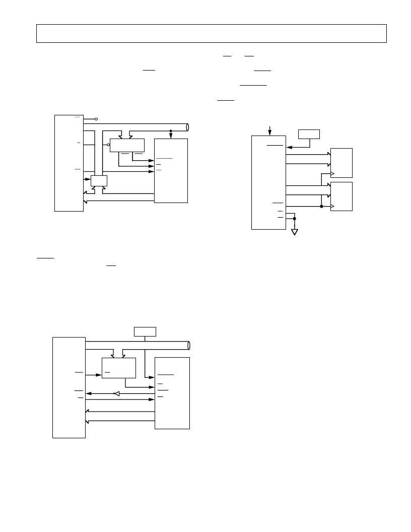
AD7885 to 8088 Interface
T he AD7885, with its byte (8 + 8) data format, is ideal for use
with the 8088 microprocessor. Figure 20 is the interface dia-
gram. Conversion is started by enabling
CSA
. At the end of
conversion, data is read into the processor. T he read instruc-
tions are:
MOV AX , C001
Read 8 MSBs of data
MOV AX , C000
Read 8 LSBs of data
8088
AD7885
ADDRESS
DECODE LOGIC
A15 – A8
AD7 – AD0
MN/MX
+5 V
HBEN
IO/M
ALE
A0
RD
ADDRESS BUS
CONVST
CS
RD
DB7 – DB0
CSA
CSB
DATA BUS
STB
8282
Figure 20. AD7885 to 8088 Interface
AD7884 to ADSP-2101 Interface
Figure 21 shows an intcrface between the AD7884 and the
ADSP-2101. Conversion is initiated using a timer which allows
very accurate control of the sampling instant. T he AD7884
BUSY
line provides an interrupt to the ADSP-2101 when con-
version is completed. T he
RD
pulse width of the processor can
be programmed using the Data Memory Wait State Control
Register. T he result can then be read from the ADC using the
following instruction:
MR0 = DM (ADC)
where MR0 is the ADSP-2101 MR0 register, and
where
ADC is the AD7884 address.
ADDRESS
DECODE LOGIC
ADSP-2101
DMA13 – DMA0
DMD15 – DMD0
IRQn
DMS
RD
EN
TIMER
AD7884
ADDRESS BUS
DATA BUS
CONVST
CS
BUSY
RD
DB15 – DB0
Figure 21. AD7884 to ADSP-2101 Interface
Stand-Alone Operation
If
CS
and
RD
are tied permanently low on the AD7884, then,
when a conversion is completed, output data will be valid on the
rising edge of
BUSY
. T his makes the device very suitable for
stand-alone operation. All that is required to run the device is an
external
CONVST
pulse which can be supplied by a sample
timer. Figure 22 shows the AD7884 set up in this mode with the
BUSY
signal providing the clock for the 74HC574 3-state
latches.
TIMER
AD7884
CONVST
CS
RD
DB15 – DB8
BUSY
HBEN
A0
74HC574
74HC574
CLK
CLK
DB7 – DB0
Figure 22. Stand-Alone Operation
Digital Feedthrough from an Active Bus
It is very important when using the AD7884/AD7885 in a
microprocessor-based system to isolate the ADC data bus from
the active processor bus while a conversion is being executed.
T his will yield the best noise performance from the ADC.
Latches like the 74HC574 can be used to do this. If the device
is connected directly to an active bus then the converter noise
will typically increase by a factor of 30%.
相關PDF資料 |
PDF描述 |
|---|---|
| AD7885AAP | LC2MOS 16-Bit, High Speed Sampling ADCs |
| AD7885ABP | LC2MOS 16-Bit, High Speed Sampling ADCs |
| AD7885AN | LC2MOS 16-Bit, High Speed Sampling ADCs |
| AD7885BN | LC2MOS 16-Bit, High Speed Sampling ADCs |
| AD7886JP | LC2MOS 12-Bit, 750 kHz/1 MHz, Sampling ADC |
相關代理商/技術參數 |
參數描述 |
|---|---|
| AD7885AAP | 制造商:Analog Devices 功能描述:16-Bit, High Speed Sampling ADCs |
| ad7885aap-reel | 制造商:Analog Devices 功能描述: |
| AD7885ABP | 制造商:Rochester Electronics LLC 功能描述:16-BIT,BYTE O/P SAMPL.A/D - Bulk 制造商:Analog Devices 功能描述: |
| AD7885ABP-REEL | 制造商:Analog Devices 功能描述: |
| AD7885AQ | 制造商:Analog Devices 功能描述: 制造商:Analog Devices 功能描述:IC 16-BIT ADC |
發布緊急采購,3分鐘左右您將得到回復。