- 您現在的位置:買賣IC網 > PDF目錄373923 > AD7885AN (ANALOG DEVICES INC) LC2MOS 16-Bit, High Speed Sampling ADCs PDF資料下載
參數資料
| 型號: | AD7885AN |
| 廠商: | ANALOG DEVICES INC |
| 元件分類: | ADC |
| 英文描述: | LC2MOS 16-Bit, High Speed Sampling ADCs |
| 中文描述: | 1-CH 16-BIT FLASH METHOD ADC, PARALLEL ACCESS, PDIP28 |
| 封裝: | PLASTIC, DIP-28 |
| 文件頁數: | 8/16頁 |
| 文件大小: | 319K |
| 代理商: | AD7885AN |
AD7884/AD7885
REV. C
–8–
T he required +3 V reference is derived from the AD780 and
buffered by the high-speed amplifier A3 (AD845, AD817 or
equivalent). A4 is a unity gain inverter which provides the –3 V
negative reference. T he gain setting resistors are on-chip and
are factory trimmed to ensure precise tracking of V
REF+
. Figure
6 shows A3 and A4 as AD845s or AD817s. T hese have the ability
to respond to the rapidly changing reference input impedance.
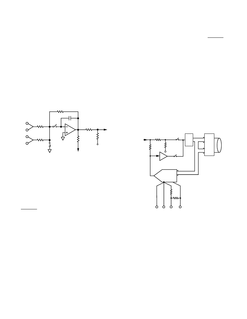
CIRCUIT DE SCRIPT ION
Analog Input Section
T he analog input section of the AD7884/AD7885 is shown in
Figure 7. It contains both the input signal conditioning and
sample-and-hold amplifier. Note that the analog input is truly
benign. When SW1a goes open circuit to put the SHA into the
hold mode, SW1b is closed. T his means that the input resis-
tors, R1 and R2 are always connected to either virtual ground
or true ground.
±
5V F
R2 5k
R1 3k
R3 3k
C1
SW1a
A1
±
5V S
±
3V F
±
3V S
R4 4k
R6 2k
R5 4k
TO RESIDUE
AMPLIFIER A2
TO
9-BIT
ADC
V
REF–
SW1b
Figure 7. AD7884/AD7885 Analog Input Section
When the
±
3 V
IN
S and
±
3 V
IN
F inputs are tied to 0 V, the in-
put section has a gain of –0.6 and transforms an input signal
of
±
5 volts to the required
±
3 volts. When the
±
5 V
IN
S and
±
5 V
IN
F inputs are grounded, the input section has a gain of
–1 and so the analog input range is now
±
3 volts. Resistors R4
and R5, at the amplifier output, further condition the
±
3 volts
signal to be 0 to –3 volts. T his is the required input for the 9-bit
A/D converter section.
With SW1a closed, the output of A1 follows the input (the
sample-and-hold is in the track mode). On the rising edge of
the
CONVST
pulse, SW1a goes open circuit, and capacitor C1
holds the voltage on the output of A1. T he sample-and-
hold is now in the hold mode. T he aperture delay time for the
sample-and-hold is nominally 50 ns.
A/D Converter Section
T he AD7884/AD7885 uses a two-pass flash technique in order
to achieve the required speed and resolution. When the
CONVST
control input goes from low to high, the sample-and-hold ampli-
fier goes into the hold mode and a 0 V to –3 V signal is pre-
sented to the input of the 9-bit ADC. T he first phase of
conversion generates the 9 MSBs of the 16-bit result and trans-
fers these to the latch and ALU combination. T hey are also fed
back to the 9 MSBs of the 16-bit DAC. T he 7 LSBs of the
DAC are permanently loaded with 0s. T he DAC output is sub-
tracted from the analog input with the result being amplified
and offset in the Residue Amplifier Section. T he signal at the
output of A2 is proportional to the error between the first phase
result and the actual analog input signal and is digitized in the
second conversion phase. T his second phase begins when the
16-bit DAC and the Residue Error Amplifier have both settled.
First, SW2 is turned off and SW3 is turned on. T hen, the SHA
section of the Residue Amplifier goes into hold mode. Next
SW2 is turned off and SW3 is turned on. T he 9-bit result is
transferred to the output latch and ALU. An error correction al-
gorithm now compensates for the offset inserted in the Residue
Amplifier Section and errors introduced in the first pass conver-
sion and combines both results to give the 16-bit answer.
9
9
V
REF–
2k
4k
4k
R4
R5
SW2
SW3
R6
A2
9-BIT
ADC
LATCH
+
ALU
16
0 TO –3V
±
3V SIGNAL
FROM INPUT
SHA
16-BIT
ACCURATE
DAC
+3V
V S
V F
V
REF–
V
INV
R7
2k
R8
2k
9
–3V
RESIDUE AMP
+
SHA
Figure 8. A/D Converter Section
相關PDF資料 |
PDF描述 |
|---|---|
| AD7885BN | LC2MOS 16-Bit, High Speed Sampling ADCs |
| AD7886JP | LC2MOS 12-Bit, 750 kHz/1 MHz, Sampling ADC |
| AD7886 | LC2MOS 12-Bit, 750 kHz/1 MHz, Sampling ADC |
| AD7886BD | LC2MOS 12-Bit, 750 kHz/1 MHz, Sampling ADC |
| AD7886KD | LC2MOS 12-Bit, 750 kHz/1 MHz, Sampling ADC |
相關代理商/技術參數 |
參數描述 |
|---|---|
| AD7885AQ | 制造商:Analog Devices 功能描述: 制造商:Analog Devices 功能描述:IC 16-BIT ADC |
| AD7885BQ | 制造商:Analog Devices 功能描述: |
| AD7885JQ | 制造商:Analog Devices 功能描述: 制造商:Rochester Electronics LLC 功能描述: |
| AD7886JD | 功能描述:IC ADC 12BIT SAMPLING HS 28-CDIP RoHS:否 類別:集成電路 (IC) >> 數據采集 - 模數轉換器 系列:- 產品培訓模塊:Lead (SnPb) Finish for COTS Obsolescence Mitigation Program 標準包裝:250 系列:- 位數:12 采樣率(每秒):1.8M 數據接口:并聯 轉換器數目:1 功率耗散(最大):1.82W 電壓電源:模擬和數字 工作溫度:-40°C ~ 85°C 安裝類型:表面貼裝 封裝/外殼:48-LQFP 供應商設備封裝:48-LQFP(7x7) 包裝:管件 輸入數目和類型:2 個單端,單極 |
| AD7886JP | 功能描述:IC ADC 12BIT SAMPLING HS 28-PLCC RoHS:否 類別:集成電路 (IC) >> 數據采集 - 模數轉換器 系列:- 標準包裝:1 系列:- 位數:14 采樣率(每秒):83k 數據接口:串行,并聯 轉換器數目:1 功率耗散(最大):95mW 電壓電源:雙 ± 工作溫度:0°C ~ 70°C 安裝類型:通孔 封裝/外殼:28-DIP(0.600",15.24mm) 供應商設備封裝:28-PDIP 包裝:管件 輸入數目和類型:1 個單端,雙極 |
發布緊急采購,3分鐘左右您將得到回復。