- 您現在的位置:買賣IC網 > PDF目錄373923 > AD7887ARM (ANALOG DEVICES INC) +2.7 V to +5.25 V, Micropower, 2-Channel, 125 kSPS, 12-Bit ADC in 8-Lead uSOIC PDF資料下載
參數資料
| 型號: | AD7887ARM |
| 廠商: | ANALOG DEVICES INC |
| 元件分類: | ADC |
| 英文描述: | +2.7 V to +5.25 V, Micropower, 2-Channel, 125 kSPS, 12-Bit ADC in 8-Lead uSOIC |
| 中文描述: | 2-CH 12-BIT SUCCESSIVE APPROXIMATION ADC, SERIAL ACCESS, PDSO8 |
| 封裝: | MO-187AA, MSOP-8 |
| 文件頁數: | 14/16頁 |
| 文件大小: | 133K |
| 代理商: | AD7887ARM |
REV. B
AD7887
–14–
MICROPROCE SSOR INT E RFACING
T he serial interface on the AD7887 allows the part to be directly
connected to a range of many different microprocessors. T his
section explains how to interface the AD7887 with some of the
more common microcontroller and DSP serial interface protocols.
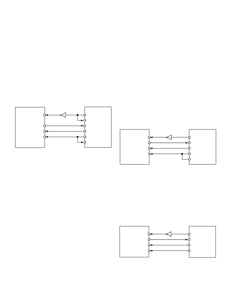
AD7887 to T MS320C5x
T he serial interface on the T MS320C5x uses a continuous serial
clock and frame synchronization signals to synchronize the data
transfer operations with peripheral devices like the AD7887.
T he
CS
input allows easy interfacing with an inverter between
the serial clock of the T MS320C5x and the AD7887 being the
only glue logic required. T he serial port of the T MS320C5x is
set up to operate in burst mode with internal CLK X (T X serial
clock) and FSX (T X frame sync). T he serial port control regis-
ter (SPC) must have the following setup: FO = 0, FSM = 1,
MCM = 1 and T X M = 1. T he connection diagram is shown in
Figure 18.
AD7887*
DOUT
DIN
SCLK
CS
TMS320C5x*
*ADDITIONAL PINS OMITTED FOR CLARITY
CLKX
CLKR
DR
DT
FSX
FSR
Figure 18. Interfacing to the TMS320C5x
AD7887 to ADSP-21xx
T he ADSP-21xx family of DSPs are easily interfaced to the
AD7887 with an inverter between the serial clock of the ADSP-
21xx and the AD7887. T his is the only glue logic required. T he
SPORT control register should be set up as follows:
T FSW = RFSW = 1, Alternate Framing
INVRFS = INVT FS = 1, Active Low Frame Signal
DT YPE = 00, Right Justify Data
SLEN = 1111, 16-Bit Data Words
ISCLK = 1, Internal Serial Clock
T FSR = RFSR = 1, Frame Every Word
IRFS = 0
IT FS = 1
T he connection diagram is shown in Figure 19. T he ADSP-
21xx has the T FS and RFS of the SPORT tied together, with
T FS set as an output and RFS set as an input. T he DSP oper-
ates in Alternate Framing Mode and the SPORT control regis-
ter is set up as described. T he Frame synchronization signal
generated on the T FS is tied to
CS
and as with all signal pro-
cessing applications equidistant sampling is necessary. In this
example however, the timer interrupt is used to control the
sampling rate of the ADC and under certain conditions, equi-
distant sampling may not be achieved.
T he T imer registers etc., are loaded with a value that will pro-
vide an interrupt at the required sample interval. When an inter-
rupt is received, a value is transmitted with T FS/DT (ADC
control word). T he T FS is used to control the RFS and hence
the reading of data. T he frequency of the serial clock is set in
the SCLK DIV register. When the instruction to transmit with
T FS is given (i.e., AX 0 = T X 0), the state of the SCL K is
checked. T he DSP will wait until the SCLK has gone High,
Low and High before transmission will start. If the timer and
SCLK values are chosen such that the instruction to transmit
occurs on or near the rising edge of SCLK , the data may be
transmitted or it may wait until the next clock edge.
For example, the ADSP-2111 has a master clock frequency of
16 MHz. If the SCLK DIV register is loaded with the value 3
then a SCLK of 2 MHz is obtained, and 8 master clock periods
will elapse for every 1 SCLK period. If the timer registers are
loaded with the value 803, then 100.5 SCLK s will occur be-
tween interrupts and subsequently between transmit instruc-
tions. T his situation will result in nonequidistant sampling as
the transmit instruction is occurring on an SCLK edge. If the
number of SCLK s between interrupts is a whole integer number
of N, equidistant sampling will be implemented by the DSP.
AD7887*
DOUT
DIN
SCLK
CS
*ADDITIONAL PINS OMITTED FOR CLARITY
SCLK
DR
DT
RFS
TFS
ADSP-21xx*
Figure 19. Interfacing to the ADSP-21xx
AD7887 to DSP56xxx
T he connection diagram in Figure 20 shows how the AD7887
can be connected to the SSI (Synchronous Serial Interface) of
the DSP56xxx family of DSPs from Motorola. T he SSI is oper-
ated in Synchronous Mode (SYN bit in CRB = 1) with inter-
nally generated 1-bit clock period frame sync for both T X and
RX (Bits FSL1 =1 and FSL0 =0 in CRB). Set the word length
to 16 by setting bits WL1 = 1 and WL0 = 0 in CRA. An inverter
is also necessary between the SCLK from the DSP56xxx and
the SCLK pin of the AD7887 as shown in Figure 20.
DOUT
DIN
SCLK
CS
*ADDITIONAL PINS OMITTED FOR CLARITY
DSP56xxx*
AD7887*
SCK
SRD
STD
SC2
Figure 20. Interfacing to the DSP56xxx
相關PDF資料 |
PDF描述 |
|---|---|
| AD7887BR | +2.7 V to +5.25 V, Micropower, 2-Channel, 125 kSPS, 12-Bit ADC in 8-Lead uSOIC |
| AD7888(中文) | 2.7 V to 5.25 V, Micro Power, 8-Channel,125kSPS,12-Bit ADC(微功耗,125kSPS,8通道12位A/D轉換器) |
| AD7888 | +2.7 V to +5.25 V, Micropower, 8-Channel, 125 kSPS, 12-Bit ADC in 16-Lead TSSOP |
| AD7888AR | +2.7 V to +5.25 V, Micropower, 8-Channel, 125 kSPS, 12-Bit ADC in 16-Lead TSSOP |
| AD7888ARU | +2.7 V to +5.25 V, Micropower, 8-Channel, 125 kSPS, 12-Bit ADC in 16-Lead TSSOP |
相關代理商/技術參數 |
參數描述 |
|---|---|
| AD7887ARM-REEL | 制造商:Analog Devices 功能描述:ADC Single SAR 125ksps 12-bit Serial 8-Pin MSOP T/R |
| AD7887ARM-REEL7 | 功能描述:IC ADC 12BIT 2CH SRL 8-MSOP RoHS:否 類別:集成電路 (IC) >> 數據采集 - 模數轉換器 系列:- 標準包裝:1,000 系列:- 位數:16 采樣率(每秒):45k 數據接口:串行 轉換器數目:2 功率耗散(最大):315mW 電壓電源:模擬和數字 工作溫度:0°C ~ 70°C 安裝類型:表面貼裝 封裝/外殼:28-SOIC(0.295",7.50mm 寬) 供應商設備封裝:28-SOIC W 包裝:帶卷 (TR) 輸入數目和類型:2 個單端,單極 |
| AD7887ARMZ | 功能描述:IC ADC 12BIT 2CH SRL 8MSOP RoHS:是 類別:集成電路 (IC) >> 數據采集 - 模數轉換器 系列:- 其它有關文件:TSA1204 View All Specifications 標準包裝:1 系列:- 位數:12 采樣率(每秒):20M 數據接口:并聯 轉換器數目:2 功率耗散(最大):155mW 電壓電源:模擬和數字 工作溫度:-40°C ~ 85°C 安裝類型:表面貼裝 封裝/外殼:48-TQFP 供應商設備封裝:48-TQFP(7x7) 包裝:Digi-Reel® 輸入數目和類型:4 個單端,單極;2 個差分,單極 產品目錄頁面:1156 (CN2011-ZH PDF) 其它名稱:497-5435-6 |
| AD7887ARMZ | 制造商:Analog Devices 功能描述:IC ADC 12BIT 125KSPS MSOP-8 |
| AD7887ARMZ-REEL | 功能描述:IC ADC 12BIT 2CH SRL 8-MSOP RoHS:是 類別:集成電路 (IC) >> 數據采集 - 模數轉換器 系列:- 標準包裝:2,500 系列:- 位數:16 采樣率(每秒):15 數據接口:MICROWIRE?,串行,SPI? 轉換器數目:1 功率耗散(最大):480µW 電壓電源:單電源 工作溫度:-40°C ~ 85°C 安裝類型:表面貼裝 封裝/外殼:38-WFQFN 裸露焊盤 供應商設備封裝:38-QFN(5x7) 包裝:帶卷 (TR) 輸入數目和類型:16 個單端,雙極;8 個差分,雙極 配用:DC1011A-C-ND - BOARD DELTA SIGMA ADC LTC2494 |
發布緊急采購,3分鐘左右您將得到回復。