- 您現(xiàn)在的位置:買賣IC網(wǎng) > PDF目錄373923 > AD7888 (Analog Devices, Inc.) +2.7 V to +5.25 V, Micropower, 8-Channel, 125 kSPS, 12-Bit ADC in 16-Lead TSSOP PDF資料下載
參數(shù)資料
| 型號: | AD7888 |
| 廠商: | Analog Devices, Inc. |
| 英文描述: | +2.7 V to +5.25 V, Micropower, 8-Channel, 125 kSPS, 12-Bit ADC in 16-Lead TSSOP |
| 中文描述: | 2.7 V至5.25 V,微功耗,8通道,125 kSPS的,12位ADC的16引腳TSSOP |
| 文件頁數(shù): | 10/16頁 |
| 文件大小: | 164K |
| 代理商: | AD7888 |
REV. 0
AD7888
–10–
order to obtain optimum performance from the device it is
advised to disable the internal reference by setting the REF bit
in the Control Register when an external reference is applied.
When the internal reference is disabled, SW1 in Figure 11 will
open and the input impedance seen at the REF IN/REF OUT
pin is the input impedance of the reference buffer, which is in
the region of giga
. When the reference is enabled, the input
impedance seen at the pin is typically 5 k
.
SW1
5k
V
2.5V
REF IN/REF OUT
Figure 11. On-Chip Reference Circuitry
Table III. Power Management Options
PM1
PM0
Mode
0
0
Normal Operation
. In this mode, the AD7888
remains in full power mode regardless of the
status of any of the logic inputs. This mode
allows the fastest possible throughput rate from
the AD7888.
0
1
Full Shutdown
. In this mode, the AD7888 is
in full shutdown mode with all circuitry on the
AD7888, including the on-chip reference, en-
tering its power-down mode. The AD7888
retains the information in the control Register
bits while in full shutdown. The part remains in
full shutdown until these bits are changed.
1
0
Autoshutdown
. In this mode, the AD7888
automatically enters full shutdown mode at the
end of each conversion. Wake-up time from full
shutdown is 5
μ
s and the user should ensure
that 5
μ
s have elapsed before attempting to
perform a valid conversion on the part in this
mode.
1
1
Autostandby
. In this standby mode, portions
of the AD7888 are powered down but the on-
chip reference voltage remains powered up. The
REF bit should be 0 to ensure the on-chip refer-
ence is enabled. This mode is similar to auto-
shutdown but allows the part to power-up much
faster.
POWER-DOWN OPTIONS
The AD7888 provides flexible power management to allow the
user to achieve the best power performance for a given through-
put rate.
The power management options are selected by programming
the power management bits (i.e., PM1 and PM0) in the control
register. Table III summarizes the options available. When the
power management bits are programmed for either of the auto
power-down modes, the part will enter the power-down mode
on the 16th rising SCLK edge after the falling edge of
CS
. The
first falling SCLK edge after the
CS
falling edge will cause the
part to power up again. When the AD7888 is in full shutdown,
the only way to fully power it up again is to reprogram the
power management bits to PM1 = PM0 = 0, i.e., normal
mode. In this case the device will power up on the 16th SCLK
rising edge after the
CS
falling edge as this is when the power
management bits become effective.
Power-Up Times
The AD7888 has an approximate 1
μ
s power-up time when
powering up from standby or when using an external reference.
When V
DD
is first connected, the AD7888 will fully power up,
i.e., it powers up in normal mode. If the part is put into shut-
down, a subsequent power-up will take approximately 5
μ
s. The
AD7888 wake-up time is very short in the autostandby mode so
it is possible to wake up the part and carry out a valid conver-
sion in the same read/write operation.
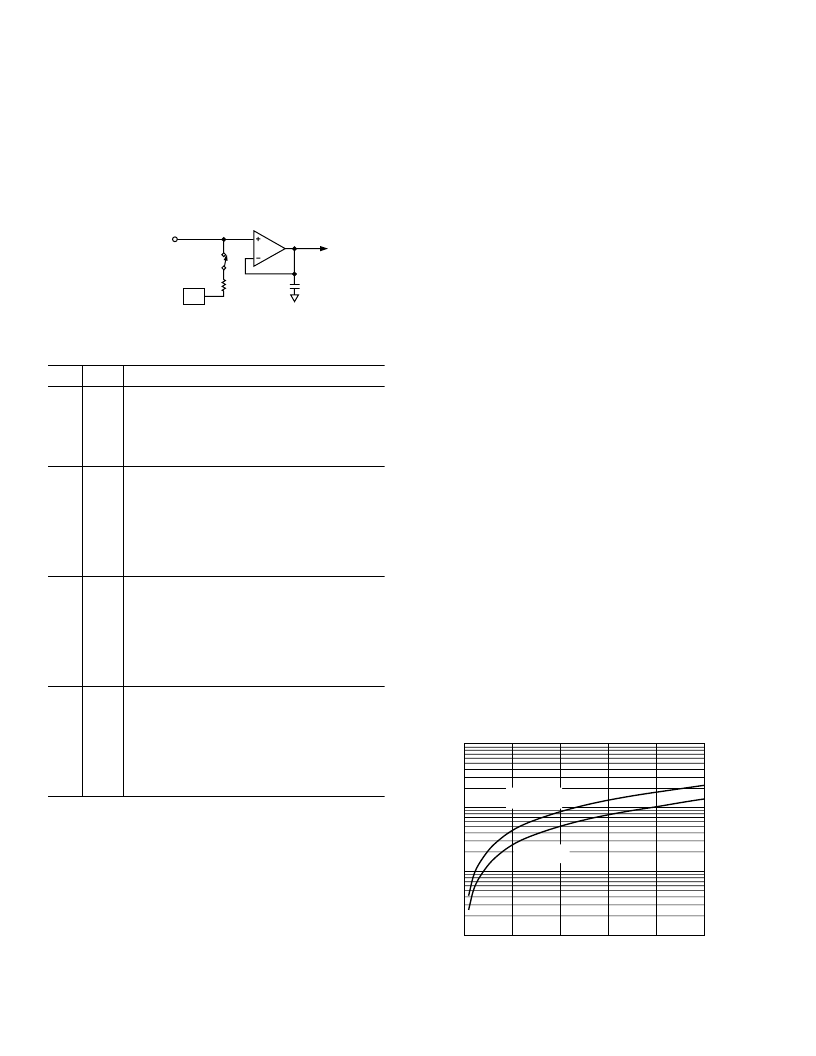
POWER VS. THROUGHPUT RATE
By operating the AD7888 in autoshutdown or autostandby
mode the average power consumption of the AD7888 decreases
at lower throughput rates. Figure 12 shows how as the through-
put rate is reduced, the device remains in its power-down state
longer and the average power consumption over time drops
accordingly.
For example, if the AD7888 were operated in a continuous
sampling mode, with a throughput rate of 10 kSPS and a SCLK
of 2 MHz (V
DD
= 5 V), and if PM1 = 1 and PM0 = 0, i.e., the
device is in autoshutdown mode and the on-chip reference is
used, the power consumption is calculated as follows. The
power dissipation during normal operation is 3.5 mW (V
DD
=
5 V). If the power-up time is 5
μ
s and the remaining conversion-
plus-acquisition time is 15.5 t
SCLK
, i.e., approximately 7.75
μ
s,
(see Figure 14a), the AD7888 can be said to dissipate 3.5 mW
for 12.75
μ
s during each conversion cycle. If the throughput rate
is 10 kSPS, the cycle time is 100
μ
s and the average power dissi-
pated during each cycle is (12.75/100)
×
(3.5 mW) = 446.25
μ
W.
If V
DD
= 3 V SCLK = 2 MHz, and the device is again in auto-
shutdown mode using the on-chip reference, the power dissipa-
tion during normal operation is 2.1 mW. The AD7888 can now
be said to dissipate 2.1 mW for 12.75
μ
s during each conversion
cycle. With a throughput rate of 10 kSPS, the average power
dissipated during each cycle is (12.75/100)
×
(2.1 mW) =
267.75
μ
W. Figure 12 shows the power vs. throughput rate for
automatic shutdown with both 5 V and 3 V supplies.
THROUGHPUT – kSPS
10
0
P
1
10
0.1
0.01
V
= +5V
SCLK = 2MHz
V
= +3V
SCLK = 2MHz
20
30
40
50
Figure 12. Power vs. Throughput
相關(guān)PDF資料 |
PDF描述 |
|---|---|
| AD7888AR | +2.7 V to +5.25 V, Micropower, 8-Channel, 125 kSPS, 12-Bit ADC in 16-Lead TSSOP |
| AD7888ARU | +2.7 V to +5.25 V, Micropower, 8-Channel, 125 kSPS, 12-Bit ADC in 16-Lead TSSOP |
| AD7888BR | +2.7 V to +5.25 V, Micropower, 8-Channel, 125 kSPS, 12-Bit ADC in 16-Lead TSSOP |
| AD7888BRU | +2.7 V to +5.25 V, Micropower, 8-Channel, 125 kSPS, 12-Bit ADC in 16-Lead TSSOP |
| AD7889 | 12-Bit 600 kSPS ADC(單電源600kSPS12位A/D轉(zhuǎn)換器) |
相關(guān)代理商/技術(shù)參數(shù) |
參數(shù)描述 |
|---|---|
| AD7888AR | 制造商:Analog Devices 功能描述:ADC Single SAR 125ksps 12-bit Serial 16-Pin SOIC N 制造商:Analog Devices 功能描述:IC 12BIT ADC 8CH MICROPOWER 7888 |
| AD7888AR-REEL | 制造商:Analog Devices 功能描述:ADC Single SAR 125ksps 12-bit Serial 16-Pin SOIC N T/R |
| AD7888AR-REEL7 | 制造商:Analog Devices 功能描述:ADC Single SAR 125ksps 12-bit Serial 16-Pin SOIC N T/R |
| AD7888ARU | 功能描述:IC ADC 12BIT 8CH 125KSPS 16TSSOP RoHS:否 類別:集成電路 (IC) >> 數(shù)據(jù)采集 - 模數(shù)轉(zhuǎn)換器 系列:- 標(biāo)準(zhǔn)包裝:1,000 系列:- 位數(shù):12 采樣率(每秒):300k 數(shù)據(jù)接口:并聯(lián) 轉(zhuǎn)換器數(shù)目:1 功率耗散(最大):75mW 電壓電源:單電源 工作溫度:0°C ~ 70°C 安裝類型:表面貼裝 封裝/外殼:24-SOIC(0.295",7.50mm 寬) 供應(yīng)商設(shè)備封裝:24-SOIC 包裝:帶卷 (TR) 輸入數(shù)目和類型:1 個單端,單極;1 個單端,雙極 |
| AD7888ARU-REEL | 功能描述:IC ADC 12BIT 8CH SRL 16-TSSOP RoHS:否 類別:集成電路 (IC) >> 數(shù)據(jù)采集 - 模數(shù)轉(zhuǎn)換器 系列:- 標(biāo)準(zhǔn)包裝:1,000 系列:- 位數(shù):16 采樣率(每秒):45k 數(shù)據(jù)接口:串行 轉(zhuǎn)換器數(shù)目:2 功率耗散(最大):315mW 電壓電源:模擬和數(shù)字 工作溫度:0°C ~ 70°C 安裝類型:表面貼裝 封裝/外殼:28-SOIC(0.295",7.50mm 寬) 供應(yīng)商設(shè)備封裝:28-SOIC W 包裝:帶卷 (TR) 輸入數(shù)目和類型:2 個單端,單極 |
發(fā)布緊急采購,3分鐘左右您將得到回復(fù)。