- 您現在的位置:買賣IC網 > PDF目錄373923 > AD7890BN-10 (ANALOG DEVICES INC) SECURITY GUARD BLACK LOCKDOWN PDF資料下載
參數資料
| 型號: | AD7890BN-10 |
| 廠商: | ANALOG DEVICES INC |
| 元件分類: | ADC |
| 英文描述: | SECURITY GUARD BLACK LOCKDOWN |
| 中文描述: | 8-CH 12-BIT PROPRIETARY METHOD ADC, SERIAL ACCESS, PDIP24 |
| 封裝: | 0.300 INCH, PLASTIC, MS-001, DIP-24 |
| 文件頁數: | 11/20頁 |
| 文件大小: | 302K |
| 代理商: | AD7890BN-10 |
AD7890
–11–
REV. A
SCLK (O)
CONVST (I)
THREE-STATE
RFS (O)
DATA OUT (O)
TRACK/HOLD
GOES INTO HOLD
t
CONVERT
NOTE
(I) SIGNIFIES AN INPUT; (O) SIGNIFIES AN OUTPUT. PULL-UP RESISTOR ON SCLK.
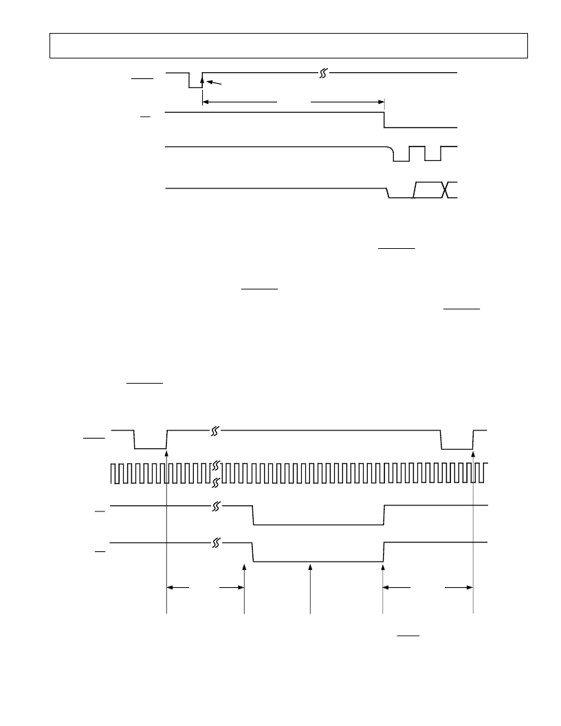
Figure 4. Self-Clocking {Master) Mode Conversion Sequence
When using the device in the External-Clocking Mode, the out-
put register can be read at any time and the most up-to-date
conversion result will be obtained. However, reading data from
the output register or writing data to the Control Register dur-
ing conversion or during the 500 ns prior to the next
CONVST
will result in reduced performance from the part. A read opera-
tion to the output register has most effect on performance with
the signal-to-noise ratio likely to degrade especially when higher
serial clock rates are used while the code flicker from the part
will also increase (see AD7890 Performance section).
Figure 5 shows the timing and control sequence required to
obtain optimum performance from the part in the external
clocking mode. In the sequence shown, conversion is initiated
on the rising edge of
CONVST
and new data is available in the
output register of the AD7890 5.9
μ
s later. Once the read oper-
ation has taken place, a further 500 ns should be allowed before
the next rising edge of
CONVST
to optimize the settling of the
track/hold before the next conversion is initiated. T he diagram
shows the read operation and the write operation taking place in
parallel. On the sixth falling edge of SCLK in the write sequence
the internal pulse will be initiated. Assuming MUX OUT is
connected to SHA IN, 2
μ
s are required between this sixth fall-
ing edge of SCLK and the rising edge of
CONVST
to allow for
the full acquisition time of the track/hold amplifier. With the
serial clock rate at its maximum of 10 MHz, the achievable
throughput rate for the part is 5.9
μ
s (conversion time) plus
0.6
μ
s (six serial clock pulses before internal pulse is initiated)
plus 2
μ
s (acquisition time). T his results in a minimum through-
put time of 8.5
μ
s (equivalent to a throughput rate of 117 kHz).
If the part is operated with a slower serial clock, it will impact
the achievable throughput rate for optimum performance.
SCLK
CONVST
CONVERSION IS
INITIATED AND
TRACK/HOLD GOES
INTO HOLD
CONVERSION
ENDS 5.9
μ
s
LATER
SERIAL READ
& WRITE
OPERATIONS
READ & WRITE
OPERATIONS SHOULD END
500ns PRIOR TO NEXT
RISING EDGE OF CONVST
RFS
TFS
NEXT
CONVERSION
START COMMAND
t
CONVERT
500ns MIN
Figure 5. External Clocking (Slave) Mode Timing
Sequence for Optimum Performance
相關PDF資料 |
PDF描述 |
|---|---|
| AD7890BN-2 | Slide Switch; Circuitry:SPDT; Contact Current Max:4A; Switch Operation:On-On; Switch Terminals:Through Hole; Actuator Style:Vertical Flush; Leaded Process Compatible:Yes; Mounting Type:PCB; Switch Features:Vertical Flush Actuator RoHS Compliant: Yes |
| AD7890BN-4 | Slide Switch; Circuitry:SPDT; Contact Current Max:4A; Switch Operation:On-On; Switch Terminals:Through Hole; Leaded Process Compatible:Yes; Mounting Type:PCB; Switch Features:Vertical Actuator RoHS Compliant: Yes |
| AD7890BR-10 | LC2MOS 8-Channel, 12-Bit Serial, Data Acquisition System |
| AD7890BR-2 | LC2MOS 8-Channel, 12-Bit Serial, Data Acquisition System |
| AD7890BR-4 | LC2MOS 8-Channel, 12-Bit Serial, Data Acquisition System |
相關代理商/技術參數 |
參數描述 |
|---|---|
| AD7890BN-2 | 制造商:Analog Devices 功能描述:ADC Single SAR 117ksps 12-bit Serial 24-Pin PDIP 制造商:Rochester Electronics LLC 功能描述:8-CH,100K,12-BIT ADC - Bulk |
| AD7890BN-4 | 制造商:Analog Devices 功能描述:ADC Single SAR 117ksps 12-bit Serial 24-Pin PDIP |
| AD7890BNZ-10 | 功能描述:IC DAS 12BIT 8CH 24-DIP RoHS:是 類別:集成電路 (IC) >> 數據采集 - ADCs/DAC - 專用型 系列:- 產品培訓模塊:Lead (SnPb) Finish for COTS Obsolescence Mitigation Program 標準包裝:50 系列:- 類型:數據采集系統(DAS) 分辨率(位):16 b 采樣率(每秒):21.94k 數據接口:MICROWIRE?,QSPI?,串行,SPI? 電壓電源:模擬和數字 電源電壓:1.8 V ~ 3.6 V 工作溫度:-40°C ~ 85°C 安裝類型:表面貼裝 封裝/外殼:40-WFQFN 裸露焊盤 供應商設備封裝:40-TQFN-EP(6x6) 包裝:托盤 |
| AD7890BNZ-2 | 功能描述:IC DAS 12BIT 8CH 24-DIP RoHS:是 類別:集成電路 (IC) >> 數據采集 - ADCs/DAC - 專用型 系列:- 產品培訓模塊:Lead (SnPb) Finish for COTS Obsolescence Mitigation Program 標準包裝:50 系列:- 類型:數據采集系統(DAS) 分辨率(位):16 b 采樣率(每秒):21.94k 數據接口:MICROWIRE?,QSPI?,串行,SPI? 電壓電源:模擬和數字 電源電壓:1.8 V ~ 3.6 V 工作溫度:-40°C ~ 85°C 安裝類型:表面貼裝 封裝/外殼:40-WFQFN 裸露焊盤 供應商設備封裝:40-TQFN-EP(6x6) 包裝:托盤 |
| AD7890BNZ-4 | 功能描述:IC DAS 12BIT 8CH 24-DIP RoHS:是 類別:集成電路 (IC) >> 數據采集 - ADCs/DAC - 專用型 系列:- 產品培訓模塊:Lead (SnPb) Finish for COTS Obsolescence Mitigation Program 標準包裝:50 系列:- 類型:數據采集系統(DAS) 分辨率(位):16 b 采樣率(每秒):21.94k 數據接口:MICROWIRE?,QSPI?,串行,SPI? 電壓電源:模擬和數字 電源電壓:1.8 V ~ 3.6 V 工作溫度:-40°C ~ 85°C 安裝類型:表面貼裝 封裝/外殼:40-WFQFN 裸露焊盤 供應商設備封裝:40-TQFN-EP(6x6) 包裝:托盤 |
發布緊急采購,3分鐘左右您將得到回復。