- 您現(xiàn)在的位置:買(mǎi)賣(mài)IC網(wǎng) > PDF目錄373923 > AD7890BN-10 (ANALOG DEVICES INC) SECURITY GUARD BLACK LOCKDOWN PDF資料下載
參數(shù)資料
| 型號(hào): | AD7890BN-10 |
| 廠商: | ANALOG DEVICES INC |
| 元件分類(lèi): | ADC |
| 英文描述: | SECURITY GUARD BLACK LOCKDOWN |
| 中文描述: | 8-CH 12-BIT PROPRIETARY METHOD ADC, SERIAL ACCESS, PDIP24 |
| 封裝: | 0.300 INCH, PLASTIC, MS-001, DIP-24 |
| 文件頁(yè)數(shù): | 14/20頁(yè) |
| 文件大小: | 302K |
| 代理商: | AD7890BN-10 |
第1頁(yè)第2頁(yè)第3頁(yè)第4頁(yè)第5頁(yè)第6頁(yè)第7頁(yè)第8頁(yè)第9頁(yè)第10頁(yè)第11頁(yè)第12頁(yè)第13頁(yè)當(dāng)前第14頁(yè)第15頁(yè)第16頁(yè)第17頁(yè)第18頁(yè)第19頁(yè)第20頁(yè)
AD7890
–14–
REV. A
SCLK (O)
DATA IN (I)
TFS (I)
A2
A1
A0
STBY
DON'T
CARE
DON'T
CARE
CONV
t
8
t
10
t
11
t
3
t
4
DON'T
CARE
t
9
t
12
NOTE
(I) SIGNIFIES AN INPUT; (O) SIGNIFIES AN OUTPUT. PULL-UP RESISTOR ON SCLK.
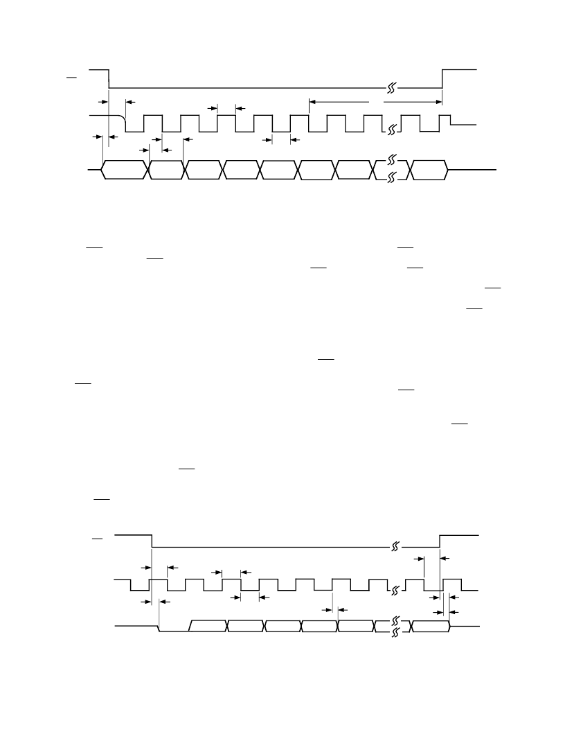
Figure 9. Self-Clocking (Master) Mode Control Register Write
Write Operation
Figure 9 shows a write operation to the Control Register of the
AD7890. T he
TFS
input is taken low to indicate to the part that
a serial write is about to occur.
TFS
going low initiates the
SCLK output and this is used to clock data out of the proces-
sors serial port and into the Control Register of the AD7890.
T he AD7890 Control Register requires only five bits of data.
T hese are loaded on the first five clock cycles of the serial clock
with data on all subsequent clock cycles being ignored. How-
ever, the part requires six serial clock cycles to load data to the
Control Register. Serial data to be written to the AD7890 must
be valid on the falling edge of SCLK .
E xternal-Clocking Mode
T he AD7890 is configured for its external clocking mode by ty-
ing the SMODE pin of the device to a logic high. In this mode,
SCLK and
RFS
of the AD7890 are configured as inputs. T his
external-clocking mode is designed for direct interface to sys-
tems which provide a serial clock output which is synchronized
to the serial data output including microcontrollers such as the
80C51, 87C51, 68HC11 and 68HC05 and most digital signal
processors.
Read Operation
Figure 10 shows the timing diagram for reading from the
AD7890 in the external-clocking mode.
RFS
goes low to access
data from the AD7890. T he serial clock input does not have to
be continuous. T he serial data can be accessed in a number of
bytes. However,
RFS
must remain low for the duration of the
data transfer operation. Once again, sixteen bits of data are
transmitted with one leading zero, followed by the three address
bits in the Control Register, followed by the 12-bit conversion
result starting with the MSB. If
RFS
goes low during the high
time of SCLK , the leading zero is clocked out from the falling
edge of
RFS
(as per Figure 10). If
RFS
goes low during the low
time of SCLK , the leading zero is clocked out on the next rising
edge of SCLK . T his ensures that, regardless of whether
RFS
goes low during a high time or low time of SCLK , the leading
zero is valid on the first falling edge of SCLK after
RFS
goes
low, provided t
14
and t
17
are adhered to. Serial data is clocked
out of the device on the rising edge of SCLK and is valid on the
falling edge of SCLK . At the end of the read operation, the
DAT A OUT line is three-stated by a rising edge on either the
SCLK or
RFS
inputs, whichever occurs first. If a serial read
from the output register is in progress when conversion is com-
plete, the updating of the output register is deferred until the
serial data read is complete and
RFS
returns high.
Write Operation
Figure 11 shows a write operation to the Control Register of the
AD7890. As with the Self-Clocking mode, the
TFS
input goes
low to indicate to the part that a serial write is about to occur.
As before, the AD7890 Control Register requires only five bits
of data. T hese are loaded on the first five clock cycles of the se-
rial clock with data on all subsequent clock cycles being ignored.
However, the part requires six serial clocks to load data to the
Control Register. Serial data to be written to the AD7890 must
be valid on the falling edge of SCLK .
LEADING
ZERO
DATA OUT (O)
SCLK (I)
3-STATE
RFS (I)
DB0
DB10
DB11
A0
A1
A2
t
13
t
15
t
16
t
17
t
18
t
19A
t
14
t
19
NOTE
(I) SIGNIFIES AN INPUT; (O) SIGNIFIES AN OUTPUT
Figure 10. External Clocking (Slave) Mode Output Register Read
相關(guān)PDF資料 |
PDF描述 |
|---|---|
| AD7890BN-2 | Slide Switch; Circuitry:SPDT; Contact Current Max:4A; Switch Operation:On-On; Switch Terminals:Through Hole; Actuator Style:Vertical Flush; Leaded Process Compatible:Yes; Mounting Type:PCB; Switch Features:Vertical Flush Actuator RoHS Compliant: Yes |
| AD7890BN-4 | Slide Switch; Circuitry:SPDT; Contact Current Max:4A; Switch Operation:On-On; Switch Terminals:Through Hole; Leaded Process Compatible:Yes; Mounting Type:PCB; Switch Features:Vertical Actuator RoHS Compliant: Yes |
| AD7890BR-10 | LC2MOS 8-Channel, 12-Bit Serial, Data Acquisition System |
| AD7890BR-2 | LC2MOS 8-Channel, 12-Bit Serial, Data Acquisition System |
| AD7890BR-4 | LC2MOS 8-Channel, 12-Bit Serial, Data Acquisition System |
相關(guān)代理商/技術(shù)參數(shù) |
參數(shù)描述 |
|---|---|
| AD7890BN-2 | 制造商:Analog Devices 功能描述:ADC Single SAR 117ksps 12-bit Serial 24-Pin PDIP 制造商:Rochester Electronics LLC 功能描述:8-CH,100K,12-BIT ADC - Bulk |
| AD7890BN-4 | 制造商:Analog Devices 功能描述:ADC Single SAR 117ksps 12-bit Serial 24-Pin PDIP |
| AD7890BNZ-10 | 功能描述:IC DAS 12BIT 8CH 24-DIP RoHS:是 類(lèi)別:集成電路 (IC) >> 數(shù)據(jù)采集 - ADCs/DAC - 專(zhuān)用型 系列:- 產(chǎn)品培訓(xùn)模塊:Lead (SnPb) Finish for COTS Obsolescence Mitigation Program 標(biāo)準(zhǔn)包裝:50 系列:- 類(lèi)型:數(shù)據(jù)采集系統(tǒng)(DAS) 分辨率(位):16 b 采樣率(每秒):21.94k 數(shù)據(jù)接口:MICROWIRE?,QSPI?,串行,SPI? 電壓電源:模擬和數(shù)字 電源電壓:1.8 V ~ 3.6 V 工作溫度:-40°C ~ 85°C 安裝類(lèi)型:表面貼裝 封裝/外殼:40-WFQFN 裸露焊盤(pán) 供應(yīng)商設(shè)備封裝:40-TQFN-EP(6x6) 包裝:托盤(pán) |
| AD7890BNZ-2 | 功能描述:IC DAS 12BIT 8CH 24-DIP RoHS:是 類(lèi)別:集成電路 (IC) >> 數(shù)據(jù)采集 - ADCs/DAC - 專(zhuān)用型 系列:- 產(chǎn)品培訓(xùn)模塊:Lead (SnPb) Finish for COTS Obsolescence Mitigation Program 標(biāo)準(zhǔn)包裝:50 系列:- 類(lèi)型:數(shù)據(jù)采集系統(tǒng)(DAS) 分辨率(位):16 b 采樣率(每秒):21.94k 數(shù)據(jù)接口:MICROWIRE?,QSPI?,串行,SPI? 電壓電源:模擬和數(shù)字 電源電壓:1.8 V ~ 3.6 V 工作溫度:-40°C ~ 85°C 安裝類(lèi)型:表面貼裝 封裝/外殼:40-WFQFN 裸露焊盤(pán) 供應(yīng)商設(shè)備封裝:40-TQFN-EP(6x6) 包裝:托盤(pán) |
| AD7890BNZ-4 | 功能描述:IC DAS 12BIT 8CH 24-DIP RoHS:是 類(lèi)別:集成電路 (IC) >> 數(shù)據(jù)采集 - ADCs/DAC - 專(zhuān)用型 系列:- 產(chǎn)品培訓(xùn)模塊:Lead (SnPb) Finish for COTS Obsolescence Mitigation Program 標(biāo)準(zhǔn)包裝:50 系列:- 類(lèi)型:數(shù)據(jù)采集系統(tǒng)(DAS) 分辨率(位):16 b 采樣率(每秒):21.94k 數(shù)據(jù)接口:MICROWIRE?,QSPI?,串行,SPI? 電壓電源:模擬和數(shù)字 電源電壓:1.8 V ~ 3.6 V 工作溫度:-40°C ~ 85°C 安裝類(lèi)型:表面貼裝 封裝/外殼:40-WFQFN 裸露焊盤(pán) 供應(yīng)商設(shè)備封裝:40-TQFN-EP(6x6) 包裝:托盤(pán) |
發(fā)布緊急采購(gòu),3分鐘左右您將得到回復(fù)。