- 您現在的位置:買賣IC網 > PDF目錄373923 > AD7890SQ-10 (ANALOG DEVICES INC) 20 Characters x 4 Lines, 5x7 Dot Matrix Character and Cursor PDF資料下載
參數資料
| 型號: | AD7890SQ-10 |
| 廠商: | ANALOG DEVICES INC |
| 元件分類: | ADC |
| 英文描述: | 20 Characters x 4 Lines, 5x7 Dot Matrix Character and Cursor |
| 中文描述: | 8-CH 12-BIT PROPRIETARY METHOD ADC, SERIAL ACCESS, CDIP24 |
| 封裝: | 0.300 INCH, CERDIP-24 |
| 文件頁數: | 15/20頁 |
| 文件大小: | 302K |
| 代理商: | AD7890SQ-10 |
AD7890
–15–
REV. A
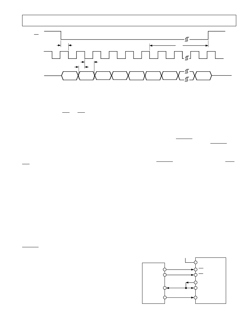
SCLK (I)
DATA IN (I)
TFS (I)
A2
A1
A0
STBY
DON'T
CARE
DON'T
CARE
CONV
t
20
t
21
t
22
DON'T
CARE
t
23
NOTE
(I) SIGNIFIES AN INPUT; (O) SIGNIFIES AN OUTPUT.
Figure 11. External Clocking (Slave) Mode Control Register Write
SIMPLIFY ING T HE INT E RFACE
T o minimize the number of interconnect lines to the AD7890,
the user can connect the
RFS
and
TFS
lines of the AD7890
together and read and write from the part simultaneously. In
this case, new control register data should be provided on the
DAT A IN line selecting the input channel and possibly provid-
ing a conversion start command while the part provides the
result from the conversion just completed on the DAT A OUT
line.
In the self-clocking mode, this means that the part provides all
the signals for the serial interface. It does require that the
microprocessor has the data to be written to the Control
Register available in its output register when the part brings the
TFS
line low. In the external clocking mode, it means that the
user only has to supply a single frame synchronization signal to
control both the read and write operations.
Care must be taken with this scheme that the read operation is
completed before the next conversion starts if the user wants to
obtain optimum performance from the part. In the case of the
software conversion start, the conversion command is written to
the Control Register on the sixth serial clock edge. However, the
read operation continues for another 10 serial clock cycles. T o
avoid reading during the sampling instant or during conversion,
the user should ensure that the internal pulse width is suffi-
ciently long (by choosing C
EX T
) so that the read operation is
completed before the next conversion sequence begins. Failure
to do this will result in significantly degraded performance from
the part, both in terms of signal-to-noise ratio and dc param-
eters. In the case of a hardware conversion start, the user should
ensure that the delay between the sixth falling edge of the serial
clock in the write operation and the next rising edge of
CONVST
is greater than the internal pulse width.
MICROPROCE SSOR/MICROCONT ROLLE R INT E RFACE
T he AD7890’s flexible serial interface allows for easy connec-
tion to the serial ports of DSP processors and microcontrollers.
Figures 12 through 15 show the AD7890 interfaced to a num-
ber of different microcontrollers and DSP processors. In some
of the interfaces shown, the AD7890 is configured as the master
in the system, providing the serial clock and frame sync for the
read operation while in others it acts as a slave with these signals
provided by the microprocessor.
AD7890–8051 Interface
Figure 12 shows an interface between the AD7890 and the
8X C51 microcontroller. T he AD7890 is configured for its ex-
ternal clocking mode while the 8X C51 is configured for its
Mode 0 serial interface mode. T he diagram shown in Figure 12
makes no provisions for monitoring when conversion is complete
on the AD7890 (assuming hardware conversion start is used).
T o monitor the conversion time on the AD7890 a scheme such
as outlined previously with
CONVST
can be used. T his can be
implemented in two ways. One is to connect the
CONVST
line
to another parallel port bit which is configured as an input. T his
port bit can then be polled to determine when conversion is
complete. An alternative is to use an interrupt driven system in
which case the
CONVST
line should be connected to the
INT1
input of the 8X C51.
Since the 8X C51 contains only one serial data line, the DAT A
OUT and DAT A IN lines of the AD7890 must be connected to-
gether. T his means that the 8X C51 cannot communicate with
the output register and Control Register of the AD7890 at the
same time. T he 8X C51 outputs the LSB first in a write opera-
tion so care should be taken in arranging the data which is to be
transmitted to the AD7890. Similarly, the AD7890 outputs the
MSB first during a read operation while the 8X C51 expects the
LSB first. T herefore, the data that is to be read into the serial
port needs to be rearranged before the correct data word from
the AD7890 is available in the microcontroller.
T he serial clock rate from the 8X C51 is limited to significantly
less than the allowable input serial clock frequency with which
the AD7890 can operate. As a result, the time to read data from
the part will actually be longer than the conversion time of the
part. T his means that the AD7890 cannot run at its maximum
throughput rate when used with the 8X C51.
SMODE
TFS
DATA OUT
DATA IN
SCLK
AD7890
RFS
P1.0
P1.1
P3.0
P3.1
8XC51
V
DD
Figure 12. AD7890 to 8XC51 Interface
相關PDF資料 |
PDF描述 |
|---|---|
| AD7890SQ-2 | 20 Characters x 4 Lines, 5x7 Dot Matrix Character and Cursor |
| AD7890SQ-4 | 20 Characters x 4 Lines, 5x7 Dot Matrix Character and Cursor |
| AD7890AN-2 | Explosion-Proof Limit Switches Series CX: Standard Housing: Side Rotary, Lever not included |
| AD7890AN-4 | Explosion-Proof Limit Switches Series CX: Standard Housing: Side Rotary, Lever not included |
| AD7891YS-1 | LC2MOS 8-Channel, 12-Bit High Speed Data Acquisition System |
相關代理商/技術參數 |
參數描述 |
|---|---|
| AD7890SQ-2 | 功能描述:模數轉換器 - ADC LC2MOS 8CH 12B Data Acquisition System RoHS:否 制造商:Analog Devices 通道數量: 結構: 轉換速率: 分辨率: 輸入類型: 信噪比: 接口類型: 工作電源電壓: 最大工作溫度: 安裝風格: 封裝 / 箱體: |
| AD7890SQ-4 | 功能描述:模數轉換器 - ADC LC2MOS 8CH 12B Data Acquisition System RoHS:否 制造商:Analog Devices 通道數量: 結構: 轉換速率: 分辨率: 輸入類型: 信噪比: 接口類型: 工作電源電壓: 最大工作溫度: 安裝風格: 封裝 / 箱體: |
| AD7891AP1 | 制造商:Analog Devices 功能描述: |
| AD7891AP-1 | 功能描述:IC DAS 12BIT 8CH 44-PLCC RoHS:否 類別:集成電路 (IC) >> 數據采集 - ADCs/DAC - 專用型 系列:- 產品培訓模塊:Lead (SnPb) Finish for COTS Obsolescence Mitigation Program 標準包裝:50 系列:- 類型:數據采集系統(DAS) 分辨率(位):16 b 采樣率(每秒):21.94k 數據接口:MICROWIRE?,QSPI?,串行,SPI? 電壓電源:模擬和數字 電源電壓:1.8 V ~ 3.6 V 工作溫度:-40°C ~ 85°C 安裝類型:表面貼裝 封裝/外殼:40-WFQFN 裸露焊盤 供應商設備封裝:40-TQFN-EP(6x6) 包裝:托盤 |
| AD7891AP-1REEL | 功能描述:IC DAS 12BIT 8CH 44-PLCC RoHS:否 類別:集成電路 (IC) >> 數據采集 - ADCs/DAC - 專用型 系列:- 產品培訓模塊:Lead (SnPb) Finish for COTS Obsolescence Mitigation Program 標準包裝:50 系列:- 類型:數據采集系統(DAS) 分辨率(位):16 b 采樣率(每秒):21.94k 數據接口:MICROWIRE?,QSPI?,串行,SPI? 電壓電源:模擬和數字 電源電壓:1.8 V ~ 3.6 V 工作溫度:-40°C ~ 85°C 安裝類型:表面貼裝 封裝/外殼:40-WFQFN 裸露焊盤 供應商設備封裝:40-TQFN-EP(6x6) 包裝:托盤 |
發布緊急采購,3分鐘左右您將得到回復。