- 您現在的位置:買賣IC網 > PDF目錄373923 > AD7890SQ-10 (ANALOG DEVICES INC) 20 Characters x 4 Lines, 5x7 Dot Matrix Character and Cursor PDF資料下載
參數資料
| 型號: | AD7890SQ-10 |
| 廠商: | ANALOG DEVICES INC |
| 元件分類: | ADC |
| 英文描述: | 20 Characters x 4 Lines, 5x7 Dot Matrix Character and Cursor |
| 中文描述: | 8-CH 12-BIT PROPRIETARY METHOD ADC, SERIAL ACCESS, CDIP24 |
| 封裝: | 0.300 INCH, CERDIP-24 |
| 文件頁數: | 17/20頁 |
| 文件大小: | 302K |
| 代理商: | AD7890SQ-10 |
AD7890
–17–
REV. A
to which the serial data is referenced, is a delayed version of the
CLK IN signal. T he typical delay between the CLK IN and
SCLK is 20 ns and will be no more than 50 ns over supplies and
temperature. T herefore, there will still be sufficient setup time
for DAT A OUT to be clocked into the DSP on the edges of the
CLK IN signal. When writing data to the AD7890, the processor’s
data hold time is sufficiently long to cater for the delay between
the two clocks. T he AD7890’s
RFS
signal connects to both the
FSX and FSR inputs of the processor. T he processor can gener-
ate its own FSX signal so if required the interface can be modi-
fied so that the
RFS
and
TFS
signals are separated and the
processor generates the FSX signal which is connected to the
TFS
input of the AD7890.
In the scheme outlined here, the user does not have to worry
about monitoring the end of conversion. Once conversion is
complete, the AD7890 takes care of transmitting back its con-
version result to the processor. Once the sixteen bits of data
have been received by the processor into its serial shift register,
it generates an internal interrupt. Since
RFS
and
TFS
are con-
nected together, data is transmitted to the Control Register of
the AD7890 whenever the AD7890 transmits its conversion
result. T he user just has to ensure that the word to be written to
the AD7890 Control Register is set up prior to the end of con-
version. As part of the interrupt routine which recognizes that
data has been read in, the processor can set up the data which it
is going to write to the Control Register next time around.
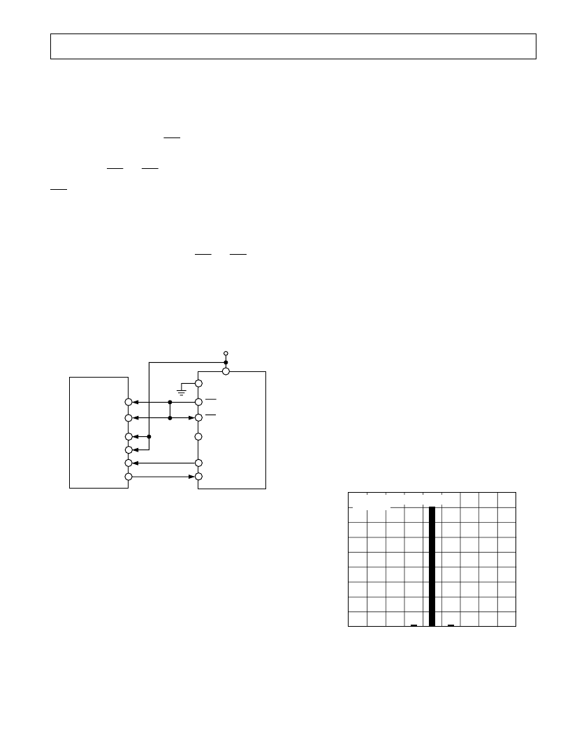
SMODE
TFS
DATA OUT
DATA IN
SCLK
AD7890
RFS
FSR
CLKX
TMS320C25/C30
DR
DX
CLKR
FSX
CLK INPUT
CLK IN
Figure 16. AD7890 to TMS320C25/30 Interface
ANT IALIASING FILT E R
T he AD7890 provides separate access to the multiplexer and
ADC via the MUX OUT and SHA IN pins. One of the reasons
for this is to allow the user to implement an antialiasing filter
between the multiplexer and the ADC. Inserting the antialiasing
filter at this point has the advantage that one antialiasing filter
can suffice for all eight channels rather than a separate antialias-
ing filter for each channel if they were to be placed prior to the
multiplexer.
T he antialiasing filter inserted between the MUX OUT and
SHA IN pins will generally be a low-pass filter to remove high
frequency signals which could possibly be aliased back in-band
during the sampling process. It is recommended that this filter is
an active filter, ideally with the MUX OUT of the AD7890 driv-
ing a high impedance stage and the SHA IN of the part being
driven from a low impedance stage. T his will remove any effects
from the variation of the part’s multiplexer on-resistance with
input signal voltage and will also remove any effects of a high
source impedance at the sampling input of the track/hold. With
an external antialiasing filter in place, the additional settling-
time associated with the filter should be accounted for by using
a larger capacitance on C
EX T
.
AD7890 PE RFORMANCE
Linearity
T he linearity of the AD7890 is primarily determined by the
on-chip 12-bit D/A converter. T his is a segmented DAC which
is laser trimmed for 12-bit integral linearity and differential lin-
earity. T ypical relative numbers for the part are
±
1/4 LSB while
the typical DNL errors are
±
1/2 LSB.
Noise
In an A/D converter, noise exhibits itself as code uncertainty in
dc applications and as the noise floor (in an FFT , for example)
in ac applications. In a sampling A/D converter like the
AD7890, all information about the analog input appears in the
baseband from dc to 1/2 the sampling frequency. T he input
bandwidth of the track/hold exceeds the Nyquist bandwidth
and, therefore, an antialiasing filter should be used to remove
unwanted signals above f
S
/2 in the input signal in applications
where such signals exist.
Figure 17 shows a histogram plot for 8192 conversions of a dc
input using the AD7890. T he analog input was set at the centre
of a code transition. T he timing and control sequence used was
as per Figure 5 where the optimum performance of the ADC
was achieved. T he same performance will be achieved in self-
clocking mode where the part transmits its data after conversion
is complete. It can be seen that almost all the codes appear in
the one output bin indicating very good noise performance from
the ADC. T he rms noise performance for the AD7890-2 for the
above plot was 81
μ
V. Since the analog input range, and hence
LSB size, on the AD7893-4 is 1.638 times what it is for the
AD7893-2, the same output code distribution results in an out-
put rms noise of 143
μ
V for the AD7893-4. For the AD7890-10,
with an LSB size eight times that of the AD7890-2, the code distri-
bution represents an output rms noise of 648
μ
V.
9000
0
2000
1000
(X–3)
(X–4)
3000
4000
5000
6000
7000
8000
(X+4)
(X+3)
(X+2)
(X+1)
X
(X–1)
(X–2)
SAMPLING FREQUENCY = 102.4kHz
T
A
= +25°C
O
CODE
Figure 17. Histogram of 8192 Conversions of a DC Input
相關PDF資料 |
PDF描述 |
|---|---|
| AD7890SQ-2 | 20 Characters x 4 Lines, 5x7 Dot Matrix Character and Cursor |
| AD7890SQ-4 | 20 Characters x 4 Lines, 5x7 Dot Matrix Character and Cursor |
| AD7890AN-2 | Explosion-Proof Limit Switches Series CX: Standard Housing: Side Rotary, Lever not included |
| AD7890AN-4 | Explosion-Proof Limit Switches Series CX: Standard Housing: Side Rotary, Lever not included |
| AD7891YS-1 | LC2MOS 8-Channel, 12-Bit High Speed Data Acquisition System |
相關代理商/技術參數 |
參數描述 |
|---|---|
| AD7890SQ-2 | 功能描述:模數轉換器 - ADC LC2MOS 8CH 12B Data Acquisition System RoHS:否 制造商:Analog Devices 通道數量: 結構: 轉換速率: 分辨率: 輸入類型: 信噪比: 接口類型: 工作電源電壓: 最大工作溫度: 安裝風格: 封裝 / 箱體: |
| AD7890SQ-4 | 功能描述:模數轉換器 - ADC LC2MOS 8CH 12B Data Acquisition System RoHS:否 制造商:Analog Devices 通道數量: 結構: 轉換速率: 分辨率: 輸入類型: 信噪比: 接口類型: 工作電源電壓: 最大工作溫度: 安裝風格: 封裝 / 箱體: |
| AD7891AP1 | 制造商:Analog Devices 功能描述: |
| AD7891AP-1 | 功能描述:IC DAS 12BIT 8CH 44-PLCC RoHS:否 類別:集成電路 (IC) >> 數據采集 - ADCs/DAC - 專用型 系列:- 產品培訓模塊:Lead (SnPb) Finish for COTS Obsolescence Mitigation Program 標準包裝:50 系列:- 類型:數據采集系統(DAS) 分辨率(位):16 b 采樣率(每秒):21.94k 數據接口:MICROWIRE?,QSPI?,串行,SPI? 電壓電源:模擬和數字 電源電壓:1.8 V ~ 3.6 V 工作溫度:-40°C ~ 85°C 安裝類型:表面貼裝 封裝/外殼:40-WFQFN 裸露焊盤 供應商設備封裝:40-TQFN-EP(6x6) 包裝:托盤 |
| AD7891AP-1REEL | 功能描述:IC DAS 12BIT 8CH 44-PLCC RoHS:否 類別:集成電路 (IC) >> 數據采集 - ADCs/DAC - 專用型 系列:- 產品培訓模塊:Lead (SnPb) Finish for COTS Obsolescence Mitigation Program 標準包裝:50 系列:- 類型:數據采集系統(DAS) 分辨率(位):16 b 采樣率(每秒):21.94k 數據接口:MICROWIRE?,QSPI?,串行,SPI? 電壓電源:模擬和數字 電源電壓:1.8 V ~ 3.6 V 工作溫度:-40°C ~ 85°C 安裝類型:表面貼裝 封裝/外殼:40-WFQFN 裸露焊盤 供應商設備封裝:40-TQFN-EP(6x6) 包裝:托盤 |
發布緊急采購,3分鐘左右您將得到回復。