- 您現在的位置:買賣IC網 > PDF目錄373923 > AD7890SQ-10 (ANALOG DEVICES INC) 20 Characters x 4 Lines, 5x7 Dot Matrix Character and Cursor PDF資料下載
參數資料
| 型號: | AD7890SQ-10 |
| 廠商: | ANALOG DEVICES INC |
| 元件分類: | ADC |
| 英文描述: | 20 Characters x 4 Lines, 5x7 Dot Matrix Character and Cursor |
| 中文描述: | 8-CH 12-BIT PROPRIETARY METHOD ADC, SERIAL ACCESS, CDIP24 |
| 封裝: | 0.300 INCH, CERDIP-24 |
| 文件頁數: | 9/20頁 |
| 文件大小: | 302K |
| 代理商: | AD7890SQ-10 |
AD7890
–9–
REV. A
tions occur on successive integer L SB values (i.e., 1 L SB,
2 L SBs, 3 L SBs . . . ). Output coding is straight (natural)
binary with 1 LSB = FS/4096 = 4.096 V/4096 = 1 mV. T he
ideal input/output transfer function is shown in T able II.
AA
AA
REFERENCE
2k
TO ADC
REFERENCE
CIRCUITRY
200
*
V
INX
AGND
MUX OUT
AD7890-4
*EQUIVALENT ON-RESISTANCE OF MULTIPLEXER
REF OUT/
REF IN
6k
9.38k
Figure 3. AD7890-4 Analog Input Structure
T able II. Ideal Input/Output Code T able for the AD7890-4
Digital Output
Code T ransition
Analog Input
1
+FSR – 1 LSB
2
(4.095 V)
+FSR – 2 LSBs (4.094 V)
+FSR – 3 LSBs (4.093 V)
AGND + 3 LSBs (0.003 V)
AGND + 2 LSBs (0.002 V)
AGND + 1 LSB (0.001 V)
111 . . . 110 to 111 . . . 111
111 . . . 101 to 111 . . . 110
111 . . . 100 to 111 . . . 101
000 . . . 010 to 000 . . . 011
000 . . . 001 to 000 . . . 010
000 . . . 000 to 000 . . . 001
NOT ES
1
FSR is full-scale range and is 4.096 V with REF IN +2.5 V.
2
1 LSB = FSR/4096 = 1 mV with REF IN = +2.5 V.
AD7890-2
T he analog input section for the AD7890-2 contains no biasing
resistors and the selected analog input connects to the multi-
plexer and in cases where MUX OUT is connected to SHA IN
this is followed by the high input impedance stage of the track/
hold amplifier. T he analog input range is, therefore, 0 V to +2.5V
into a high impedance stage with an input current of less than
50 nA. T he designed code transitions occur on successive integer
LSB values (i.e., l LSB, 2 LSBs, 3 LSBs . . . FS-1 LSBs). Out-
put coding is straight (natural) binary with 1 LSB = FS/4096 =
2.5 V/4096 = 0.61 mV. T he ideal input/output transfer function
is shown in T able III.
T able III. Ideal Input/Output Code T able for the AD7890-2
Digital Output
Code T ransition
Analog Input
1
+FSR – 1 LSB
2
(2.499390 V)
+FSR – 2 LSBs (2.498779 V)
+FSR – 3 LSBs (2.498169 V)
AGND + 3 LSBs (0.001831 V)
AGND + 2 LSBs (0.001221 V)
AGND + 1 LSB (0.000610 V)
111 . . . 110 to 111 . . . 111
111 . . . 101 to 111 . . . 110
111 . . . 100 to 111 . . . 101
000 . . . 010 to 010 . . . 011
000 . . . 001 to 001 . . . 010
000 . . . 000 to 000 . . . 001
NOT ES
1
FSR is full-scale range and is 2.5 V with REF IN = +2.5 V.
2
1 LSB = FSR/4096 = 0.61 mV with REF IN = +2.5 V.
CIRCUIT DE SCRIPT ION
Analog Input Section
T he AD7890 is offered as three part types, the AD7890-10
which handles a
±
10 V input voltage range, the AD7890-4
which handles a 0 V to +4.096 V input range and the AD7890-2
which handles a 0 V to +2.5 V input voltage range.
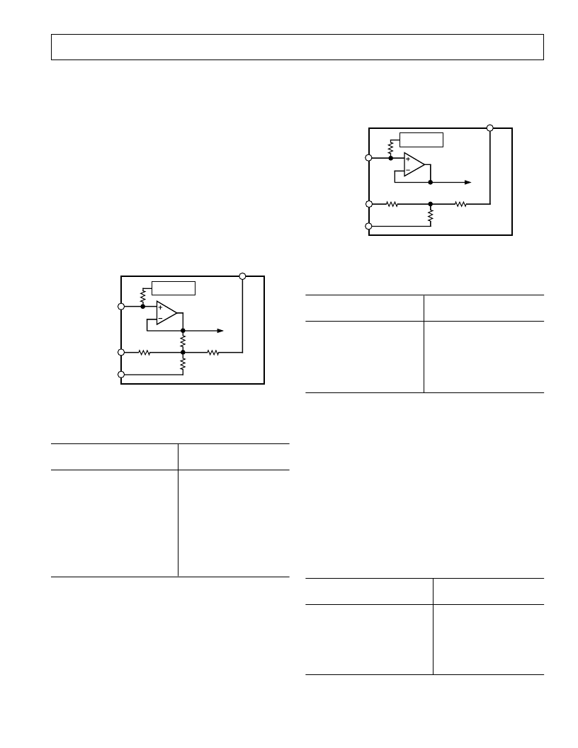
AD7890-10
Figure 2 shows the analog input section for the AD7890-10.
T he analog input range for each of the analog inputs is
±
10 V
into an input resistance of typically 33 k
. T his input is benign
with no dynamic charging currents with the resistor attenuator
stage followed by the multiplexer and in cases where MUX
OUT is connected to SHA IN this is followed by the high input
impedance stage of the track/hold amplifier. T he designed code
transitions occur on successive integer LSB values (i.e., 1 LSB,
2 LSBs, 3 LSBs...). Output coding is 2s complement binary
with 1 LSB – FS/4096 = 20 V/4096 = 4.88 mV. T he ideal input/
output transfer function is shown in T able I.
AA
AA
2k
TO ADC
REFERENCE
CIRCUITRY
7.5k
30k
200
*
10k
V
INX
AGND
MUX OUT
AD7890-10
*EQUIVALENT ON-RESISTANCE OF MULTIPLEXER
REF OUT/
REF IN
Figure 2. AD7890-10 Analog Input Structure
T able I. Ideal Input/Output Code T able for the AD7890-10
Digital Output
Code T ransition
Analog Input
1
+FSR/2 – 1 LSB
2
(9.995117 V)
+FSR/2 – 2 LSBs (9.990234 V)
+FSR/2 – 3 LSBs (9.985352 V)
AGND + 1 LSB (0.004883 V)
AGND (0.000000 V)
AGND – 1 LSB (–0.004883 V)
–FSR/2 + 3 LSBs (–9.985352 V)
–FSR/2 + 2 LSBs (–9.990234 V)
–FSR/2 + 1 LSB (–9.995117 V)
011 . . . 110 to 011 . . . 111
011 . . . 101 to 011 . . . 110
011 . . . 100 to 011 . . . 101
000 . . . 000 to 000 . . . 001
111 . . . 111 to 000 . . . 000
111 . . . 110 to 111 . . . 111
100 . . . 010 to 100 . . . 011
100 . . . 001 to 100 . . . 010
100 . . . 000 to 100 . . . 001
NOT ES
1
FSR is full-scale range and is 20 V with REF IN = +2.5 V.
2
1 LSB = FSR/4096 = 4.883 mV with REF IN = +2.5 V.
AD7890-4
Figure 3 shows the analog input section for the AD7890-4. T he
analog input range for each of the analog inputs is
±
10 V into
an input resistance of typically 15 k
. T his input is benign with
no dynamic charging currents with the resistor attenuator stage
followed by the multiplexer and in cases where MUX OUT is
connected to SHA IN this is followed by the high input imped-
ance stage of the track/hold amplifier. T he designed code transi-
相關PDF資料 |
PDF描述 |
|---|---|
| AD7890SQ-2 | 20 Characters x 4 Lines, 5x7 Dot Matrix Character and Cursor |
| AD7890SQ-4 | 20 Characters x 4 Lines, 5x7 Dot Matrix Character and Cursor |
| AD7890AN-2 | Explosion-Proof Limit Switches Series CX: Standard Housing: Side Rotary, Lever not included |
| AD7890AN-4 | Explosion-Proof Limit Switches Series CX: Standard Housing: Side Rotary, Lever not included |
| AD7891YS-1 | LC2MOS 8-Channel, 12-Bit High Speed Data Acquisition System |
相關代理商/技術參數 |
參數描述 |
|---|---|
| AD7890SQ-2 | 功能描述:模數轉換器 - ADC LC2MOS 8CH 12B Data Acquisition System RoHS:否 制造商:Analog Devices 通道數量: 結構: 轉換速率: 分辨率: 輸入類型: 信噪比: 接口類型: 工作電源電壓: 最大工作溫度: 安裝風格: 封裝 / 箱體: |
| AD7890SQ-4 | 功能描述:模數轉換器 - ADC LC2MOS 8CH 12B Data Acquisition System RoHS:否 制造商:Analog Devices 通道數量: 結構: 轉換速率: 分辨率: 輸入類型: 信噪比: 接口類型: 工作電源電壓: 最大工作溫度: 安裝風格: 封裝 / 箱體: |
| AD7891AP1 | 制造商:Analog Devices 功能描述: |
| AD7891AP-1 | 功能描述:IC DAS 12BIT 8CH 44-PLCC RoHS:否 類別:集成電路 (IC) >> 數據采集 - ADCs/DAC - 專用型 系列:- 產品培訓模塊:Lead (SnPb) Finish for COTS Obsolescence Mitigation Program 標準包裝:50 系列:- 類型:數據采集系統(DAS) 分辨率(位):16 b 采樣率(每秒):21.94k 數據接口:MICROWIRE?,QSPI?,串行,SPI? 電壓電源:模擬和數字 電源電壓:1.8 V ~ 3.6 V 工作溫度:-40°C ~ 85°C 安裝類型:表面貼裝 封裝/外殼:40-WFQFN 裸露焊盤 供應商設備封裝:40-TQFN-EP(6x6) 包裝:托盤 |
| AD7891AP-1REEL | 功能描述:IC DAS 12BIT 8CH 44-PLCC RoHS:否 類別:集成電路 (IC) >> 數據采集 - ADCs/DAC - 專用型 系列:- 產品培訓模塊:Lead (SnPb) Finish for COTS Obsolescence Mitigation Program 標準包裝:50 系列:- 類型:數據采集系統(DAS) 分辨率(位):16 b 采樣率(每秒):21.94k 數據接口:MICROWIRE?,QSPI?,串行,SPI? 電壓電源:模擬和數字 電源電壓:1.8 V ~ 3.6 V 工作溫度:-40°C ~ 85°C 安裝類型:表面貼裝 封裝/外殼:40-WFQFN 裸露焊盤 供應商設備封裝:40-TQFN-EP(6x6) 包裝:托盤 |
發布緊急采購,3分鐘左右您將得到回復。