- 您現(xiàn)在的位置:買賣IC網(wǎng) > PDF目錄373924 > AD7891AS-2 (ANALOG DEVICES INC) LC2MOS 8-Channel, 12-Bit High Speed Data Acquisition System PDF資料下載
參數(shù)資料
| 型號(hào): | AD7891AS-2 |
| 廠商: | ANALOG DEVICES INC |
| 元件分類: | ADC |
| 英文描述: | LC2MOS 8-Channel, 12-Bit High Speed Data Acquisition System |
| 中文描述: | 8-CH 12-BIT PROPRIETARY METHOD ADC, SERIAL/PARALLEL ACCESS, PQFP44 |
| 封裝: | PLASTIC, MO-112-AA-1, MQFP-44 |
| 文件頁數(shù): | 8/20頁 |
| 文件大小: | 173K |
| 代理商: | AD7891AS-2 |
AD7891
–8–
REV. A
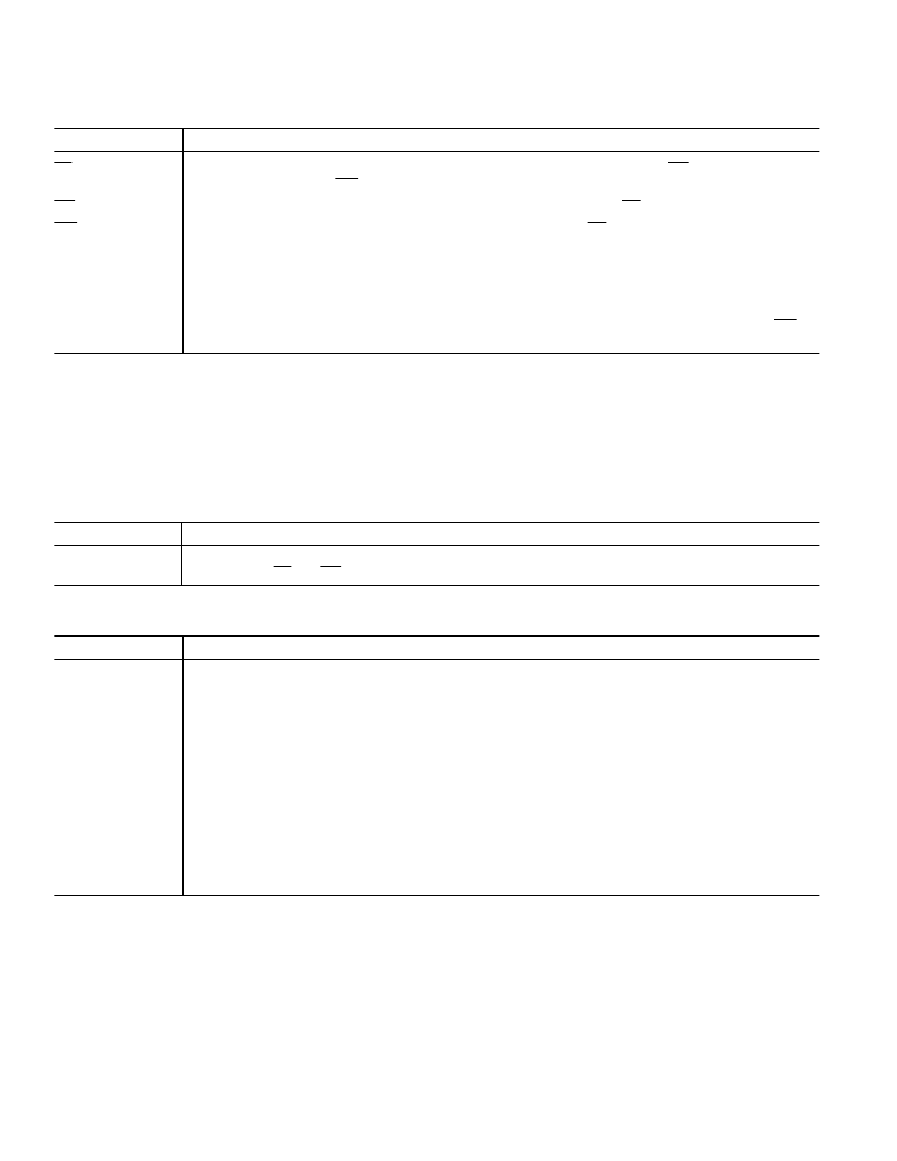
PARALLEL INTERFACE MODE FUNCTIONS
Mnemonic
Description
CS
Chip Select Input. Active low logic input which is used in conjunction with
RD
to enable the data
outputs and with
WR
to allow input data to be written to the part.
Read Input. Active low logic input which is used in conjunction with
CS
low to enable the data outputs.
Write Input. Active low, logic input used in conjunction with
CS
to latch the multiplexer address and
software control information. The rising edge of this input also initiates an internal pulse. When using
the software start facility, this pulse delays the point at which the track/hold goes into hold and con-
version is initiated. This allows the multiplexer to settle and acquisition time of the track/hold to
elapse when a channel address is changed. If the SWCON bit of the control register is set to 1, when
this pulse times out, the track/hold then goes into hold and conversion is initiated. If the SWCON bit
of the control register is set to 0 the track/hold and conversion sequence are unaffected by the
WR
operation.
RD
WR
Data I/O Lines
There are 12 data input/output lines on the AD7891. When the part is configured for parallel mode (MODE = 1), the output data
from the part is provided at these 12 pins during a read operation. For a write operation in parallel mode, these lines provide access
to the part’s Control Register.
Parallel Read Operation
During a parallel read operation the 12 lines become the 12 data bits containing the conversion result from the AD7891. These data
bits are labelled Data Bit 0 (LSB) to Data Bit 11 (MSB). They are three-state TTL-compatible outputs. Output data coding is twos
complement when the data FORMAT Bit of the control register is 1 and straight binary when the data FORMAT Bit of the control
register is 0.
Mnemonic
Description
DB0–DB11
Data Bit 0 (LSB) to Data Bit 11 (MSB). Three-state TTL-compatible outputs which are controlled
by the
CS
and
RD
inputs.
Parallel Write Operation
During a parallel write operation the following functions can be written to the control register via the 12 data input/output pins.
Mnemonic
Description
A0
Address Input. The status of this input during a parallel write operation is latched to the A0 bit of the
control register (see Control Register section).
Address Input. The status of this input during a parallel write operation is latched to the A1 bit of the
control register (see Control Register section).
Address Input. The status of this input during a parallel write operation is latched to the A2 bit of the
control register (see Control Register section).
Software Conversion Start. The status of this input during a parallel write operation is latched to the
SWCONV bit of the control register (see Control Register section).
Software Standby Control. The status of this input during a parallel write operation is latched to the
SWSTBY bit of the control register (see Control Register section).
Data Format Selection. The status of this input during a parallel write operation is latched to the
FORMAT bit of the control register (see Control Register section).
A1
A2
SWCON
SWSTBY
FORMAT
相關(guān)PDF資料 |
PDF描述 |
|---|---|
| AD7892AR-2 | LC2MOS Single Supply, 12-Bit 600 kSPS ADC |
| AD7892SQ-1 | LC2MOS Single Supply, 12-Bit 600 kSPS ADC |
| AD7892 | LC2MOS Single Supply, 12-Bit 600 kSPS ADC |
| AD7892AR | RADIATION HARDENED HIGH EFFICIENCY, 5 AMP SWITCHING REGULATORS |
| AD7892AR-3 | LC2MOS Single Supply, 12-Bit 600 kSPS ADC |
相關(guān)代理商/技術(shù)參數(shù) |
參數(shù)描述 |
|---|---|
| AD7891ASZ-1 | 功能描述:IC DAS 12BIT 8CH HI-SPD 44-MQFP RoHS:是 類別:集成電路 (IC) >> 數(shù)據(jù)采集 - ADCs/DAC - 專用型 系列:- 產(chǎn)品培訓(xùn)模塊:Data Converter Basics 標(biāo)準(zhǔn)包裝:1 系列:- 類型:電機(jī)控制 分辨率(位):12 b 采樣率(每秒):1M 數(shù)據(jù)接口:串行,并聯(lián) 電壓電源:單電源 電源電壓:2.7 V ~ 3.6 V,4.5 V ~ 5.5 V 工作溫度:-40°C ~ 85°C 安裝類型:表面貼裝 封裝/外殼:100-TQFP 供應(yīng)商設(shè)備封裝:100-TQFP(14x14) 包裝:剪切帶 (CT) 其它名稱:296-18373-1 |
| AD7891ASZ-1 | 制造商:Analog Devices 功能描述:IC 12-BIT ADC |
| AD7891ASZ-1REEL | 功能描述:IC DAS 12BIT 8CH 44-MQFP RoHS:是 類別:集成電路 (IC) >> 數(shù)據(jù)采集 - ADCs/DAC - 專用型 系列:- 產(chǎn)品培訓(xùn)模塊:Lead (SnPb) Finish for COTS Obsolescence Mitigation Program 標(biāo)準(zhǔn)包裝:50 系列:- 類型:數(shù)據(jù)采集系統(tǒng)(DAS) 分辨率(位):16 b 采樣率(每秒):21.94k 數(shù)據(jù)接口:MICROWIRE?,QSPI?,串行,SPI? 電壓電源:模擬和數(shù)字 電源電壓:1.8 V ~ 3.6 V 工作溫度:-40°C ~ 85°C 安裝類型:表面貼裝 封裝/外殼:40-WFQFN 裸露焊盤 供應(yīng)商設(shè)備封裝:40-TQFN-EP(6x6) 包裝:托盤 |
| AD7891ASZ-2 | 功能描述:IC DAS 12BIT 8CH 44-MQFP RoHS:是 類別:集成電路 (IC) >> 數(shù)據(jù)采集 - ADCs/DAC - 專用型 系列:- 產(chǎn)品培訓(xùn)模塊:Lead (SnPb) Finish for COTS Obsolescence Mitigation Program 標(biāo)準(zhǔn)包裝:50 系列:- 類型:數(shù)據(jù)采集系統(tǒng)(DAS) 分辨率(位):16 b 采樣率(每秒):21.94k 數(shù)據(jù)接口:MICROWIRE?,QSPI?,串行,SPI? 電壓電源:模擬和數(shù)字 電源電壓:1.8 V ~ 3.6 V 工作溫度:-40°C ~ 85°C 安裝類型:表面貼裝 封裝/外殼:40-WFQFN 裸露焊盤 供應(yīng)商設(shè)備封裝:40-TQFN-EP(6x6) 包裝:托盤 |
| AD7891ASZ-2REEL | 功能描述:IC DAS 12BIT 8CH 44-MQFP RoHS:是 類別:集成電路 (IC) >> 數(shù)據(jù)采集 - ADCs/DAC - 專用型 系列:- 產(chǎn)品培訓(xùn)模塊:Lead (SnPb) Finish for COTS Obsolescence Mitigation Program 標(biāo)準(zhǔn)包裝:50 系列:- 類型:數(shù)據(jù)采集系統(tǒng)(DAS) 分辨率(位):16 b 采樣率(每秒):21.94k 數(shù)據(jù)接口:MICROWIRE?,QSPI?,串行,SPI? 電壓電源:模擬和數(shù)字 電源電壓:1.8 V ~ 3.6 V 工作溫度:-40°C ~ 85°C 安裝類型:表面貼裝 封裝/外殼:40-WFQFN 裸露焊盤 供應(yīng)商設(shè)備封裝:40-TQFN-EP(6x6) 包裝:托盤 |
發(fā)布緊急采購,3分鐘左右您將得到回復(fù)。