- 您現(xiàn)在的位置:買賣IC網 > PDF目錄373926 > AD7910AKS-REEL7 (ANALOG DEVICES INC) 250 kSPS, 10-/12-Bit ADCs in 6-Lead SC70 PDF資料下載
參數資料
| 型號: | AD7910AKS-REEL7 |
| 廠商: | ANALOG DEVICES INC |
| 元件分類: | ADC |
| 英文描述: | 250 kSPS, 10-/12-Bit ADCs in 6-Lead SC70 |
| 中文描述: | 1-CH 10-BIT SUCCESSIVE APPROXIMATION ADC, SERIAL ACCESS, PDSO6 |
| 封裝: | MO-203AB, SC-70, 6 PIN |
| 文件頁數: | 16/20頁 |
| 文件大小: | 1091K |
| 代理商: | AD7910AKS-REEL7 |
REV. B
–16–
AD7910/AD7920
MICROPROCESSOR INTERFACING
The serial interface on the AD7910/AD7920 allows the part to
be directly connected to a range of different microprocessors.
This section explains how to interface the AD7910/AD7920
with some of the more common microcontroller and DSP serial
interface protocols.
AD7910/AD7920 to TMS320C541 Interface
The serial interface on the TMS320C541 uses a continuous serial
clock and frame synchronization signals to synchronize the data
transfer operations with peripheral devices like the AD7910/
AD7920. The
CS
input allows easy interfacing between the
TMS320C541 and the AD7910/AD7920 without any glue logic
required. The serial port of the TMS320C541 is set up to operate
in burst mode (FSM = 1 in the Serial Port Control register, SPC)
with internal serial clock CLKX (MCM = 1 in SPC register) and
internal frame signal (TXM = 1 in the SPC), so both pins are
configured as outputs. For the AD7920, the word length should
be set to 16 bits (FO = 0 in the SPC register). This DSP allows
frames with a word length of 16 or 8 bits. Therefore, in the case
of the AD7910 where just 14 bits could be required, the FO bit
would be set up to 16 bits also. This means that to obtain the
conversion result, 16 SCLKs are needed and two trailing zeros will
be clocked out in the two last clock cycles.
To summarize, the values in the SPC register are:
FO = 0
FSM = 1
MCM = 1
TXM = 1
The format bit, FO, may be set to 1 to set the word length to
eight bits, in order to implement the power-down mode on the
AD7910/AD7920.
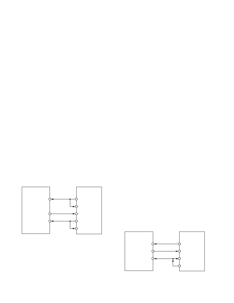
The connection diagram is shown in Figure 15. It should be noted
that for signal processing applications, it is imperative that the
frame synchronization signal from the TMS320C541 provides
equidistant sampling.
AD7910/AD7920
*
SCLK
SDATA
CS
CLKX
CLKR
FSX
FSR
TMS320C541
*
*
ADDITIONAL PINS OMITTED FOR CLARITY
DR
Figure 15. Interfacing to the TMS320C541
AD7910/AD7920 to ADSP-218x
The ADSP-218x family of DSPs is interfaced directly to the
AD7910/AD7920 without any glue logic required. The SPORT
control register should be set up as follows:
TFSW = RFSW = 1, Alternate Framing
INVRFS = INVTFS = 1, Active Low Frame Signal
DTYPE = 00, Right Justify Data
ISCLK = 1, Internal Serial Clock
TFSR = RFSR = 1, Frame Every Word
IRFS = 0, Sets up RFS as an Input
ITFS = 1, Sets up TFS as an Output
SLEN = 1111, 16 Bits for the AD7920
SLEN = 1101, 14 Bits for the AD7910
To implement power-down mode, SLEN should be set to 0111
to issue an 8-bit SCLK burst. The connection diagram is shown
in Figure 16. The ADSP-218x has the TFS and RFS of the
SPORT tied together, with TFS set as an output and RFS set as
an input. The DSP operates in alternate framing mode and the
SPORT control register is set up as described. The frame syn-
chronization signal generated on the TFS is tied to
CS
and, as
with all signal processing applications, equidistant sampling is
necessary. However, in this example, the timer interrupt is used
to control the sampling rate of the ADC and, under certain
conditions, equidistant sampling may not be achieved.
The timer registers are loaded with a value that provides an
interrupt at the required sample interval. When an interrupt is
received, a value is transmitted with TFS/DT (ADC control word).
The TFS is used to control the RFS and thus the reading of
data. The frequency of the serial clock is set in the SCLKDIV
register. When the instruction to transmit with TFS is given,
i.e., TX0 = AX0, the state of the SCLK is checked. The DSP
waits until the SCLK has gone high, low, and high before trans-
mission starts. If the timer and SCLK values are chosen such
that the instruction to transmit occurs on or near the rising edge
of SCLK, the data may be transmitted or it may wait until the
next clock edge.
For example, the ADSP-2111 has a master clock frequency of
16 MHz. If the SCLKDIV register is loaded with the value 3, an
SCLK of 2 MHz is obtained and eight master clock periods will
elapse for every one SCLK period. If the timer registers are loaded
with the value 803, 100.5 SCLKs will occur between interrupts
and subsequently between transmit instructions. This situation
will result in nonequidistant sampling as the transmit instruction
is occurring on an SCLK edge. If the number of SCLKs between
interrupts is a whole integer figure of N, equidistant sampling
will be implemented by the DSP.
AD7910/AD7920
*
SCLK
SDATA
CS
SCLK
DR
RFS
TFS
ADSP-218x
*
*
ADDITIONAL PINS OMITTED FOR CLARITY
Figure 16. Interfacing to the ADSP-218x
相關PDF資料 |
PDF描述 |
|---|---|
| AD7910ARM | 250 kSPS, 10-/12-Bit ADCs in 6-Lead SC70 |
| AD7910ARM-REEL | 250 kSPS, 10-/12-Bit ADCs in 6-Lead SC70 |
| AD7920 | 250 kSPS, 10-/12-Bit ADCs in 6-Lead SC70 |
| AD7910ARM-REEL7 | ECONOLINE: REC2.2-S_DRW(Z)/H* - 2.2W DIP Package- 1kVDC Isolation- Regulated Output- 4.5-9V, 9-18V, 18-36V, 36-72V Wide Input Range 2 : 1- UL94V-0 Package Material- Continuous Short Circiut Protection- Cost Effective- 100% Burned In- Efficiency to 84% |
| AD7920AKS-REEL | 250 kSPS, 10-/12-Bit ADCs in 6-Lead SC70 |
相關代理商/技術參數 |
參數描述 |
|---|---|
| AD7910AKSZ-500RL7 | 功能描述:IC ADC 10BIT SRL 250KSPS SC70-6 RoHS:是 類別:集成電路 (IC) >> 數據采集 - 模數轉換器 系列:- 其它有關文件:TSA1204 View All Specifications 標準包裝:1 系列:- 位數:12 采樣率(每秒):20M 數據接口:并聯(lián) 轉換器數目:2 功率耗散(最大):155mW 電壓電源:模擬和數字 工作溫度:-40°C ~ 85°C 安裝類型:表面貼裝 封裝/外殼:48-TQFP 供應商設備封裝:48-TQFP(7x7) 包裝:Digi-Reel® 輸入數目和類型:4 個單端,單極;2 個差分,單極 產品目錄頁面:1156 (CN2011-ZH PDF) 其它名稱:497-5435-6 |
| AD7910AKSZ-REEL | 功能描述:IC ADC 10BIT SRL 250KSPS SC70-6 RoHS:是 類別:集成電路 (IC) >> 數據采集 - 模數轉換器 系列:- 標準包裝:2,500 系列:- 位數:16 采樣率(每秒):15 數據接口:MICROWIRE?,串行,SPI? 轉換器數目:1 功率耗散(最大):480µW 電壓電源:單電源 工作溫度:-40°C ~ 85°C 安裝類型:表面貼裝 封裝/外殼:38-WFQFN 裸露焊盤 供應商設備封裝:38-QFN(5x7) 包裝:帶卷 (TR) 輸入數目和類型:16 個單端,雙極;8 個差分,雙極 配用:DC1011A-C-ND - BOARD DELTA SIGMA ADC LTC2494 |
| AD7910AKSZ-REEL7 | 功能描述:IC ADC 10BIT SRL 250KSPS SC70-6 RoHS:是 類別:集成電路 (IC) >> 數據采集 - 模數轉換器 系列:- 標準包裝:2,500 系列:- 位數:16 采樣率(每秒):15 數據接口:MICROWIRE?,串行,SPI? 轉換器數目:1 功率耗散(最大):480µW 電壓電源:單電源 工作溫度:-40°C ~ 85°C 安裝類型:表面貼裝 封裝/外殼:38-WFQFN 裸露焊盤 供應商設備封裝:38-QFN(5x7) 包裝:帶卷 (TR) 輸入數目和類型:16 個單端,雙極;8 個差分,雙極 配用:DC1011A-C-ND - BOARD DELTA SIGMA ADC LTC2494 |
| AD7910ARM | 制造商:Analog Devices 功能描述:ADC Single SAR 250ksps 10-bit Serial 8-Pin MSOP 制造商:Analog Devices 功能描述:IC 10BIT ADC SMD 7910 MSOP8 |
| AD7910ARM-REEL | 制造商:Analog Devices 功能描述:ADC Single SAR 250ksps 10-bit Serial 8-Pin MSOP T/R 制造商:Analog Devices 功能描述:ADC SGL SAR 250KSPS 10-BIT SERL 8MSOP - Tape and Reel |
發(fā)布緊急采購,3分鐘左右您將得到回復。