- 您現(xiàn)在的位置:買賣IC網(wǎng) > PDF目錄373927 > AD7923BRU (ANALOG DEVICES INC) Four Wall Header; No. of Contacts:60; Pitch Spacing:0.1"; No. of Rows:2; Gender:Header; Body Material:Glass-filled Polyester; Contact Plating:Nickel; Leaded Process Compatible:No; Mounting Type:Through Hole RoHS Compliant: No PDF資料下載
參數(shù)資料
| 型號: | AD7923BRU |
| 廠商: | ANALOG DEVICES INC |
| 元件分類: | ADC |
| 英文描述: | Four Wall Header; No. of Contacts:60; Pitch Spacing:0.1"; No. of Rows:2; Gender:Header; Body Material:Glass-filled Polyester; Contact Plating:Nickel; Leaded Process Compatible:No; Mounting Type:Through Hole RoHS Compliant: No |
| 中文描述: | 4-CH 12-BIT SUCCESSIVE APPROXIMATION ADC, SERIAL ACCESS, PDSO16 |
| 封裝: | MO-153AB, TSSOP-16 |
| 文件頁數(shù): | 17/20頁 |
| 文件大小: | 430K |
| 代理商: | AD7923BRU |
AD7923
–17–
REV. 0
For example, if the AD7923 is operated in a continuous sam-
pling mode, with a throughput rate of 200 kSPS and an SCLK
of 20 MHz (AV
DD
= 5 V), and the device is placed in Auto
Shutdown Mode, i.e., if PM1 = 0 and PM0 = 1, then the power
consumption is calculated as follows:
The maximum power dissipation during conversion is 13.5 mW
(I
DD
= 2.7 mA max, AV
DD
= 5 V). If the power-up time from
Auto Shutdown is one dummy cycle, i.e., 1
m
s, and the remaining
conversion time is another cycle, i.e., 800 ns, then the AD7923
can be said to dissipate 13.5 mW for 1.8
m
s during each con-
version cycle. For the remainder of the conversion cycle, 3.2
m
s,
the part remains in Shutdown. The AD7923 can be said to
dissipate 2.5
m
W for the remaining 3.2
m
s of the conversion
cycle. If the throughput rate is 200 kSPS, the cycle time is
5
m
s and the average power dissipated during each cycle is
(1.8/5)
¥
(13.5 mW) + (3.2/5)
¥
(2.5
m
W) = 4.8616 mW.
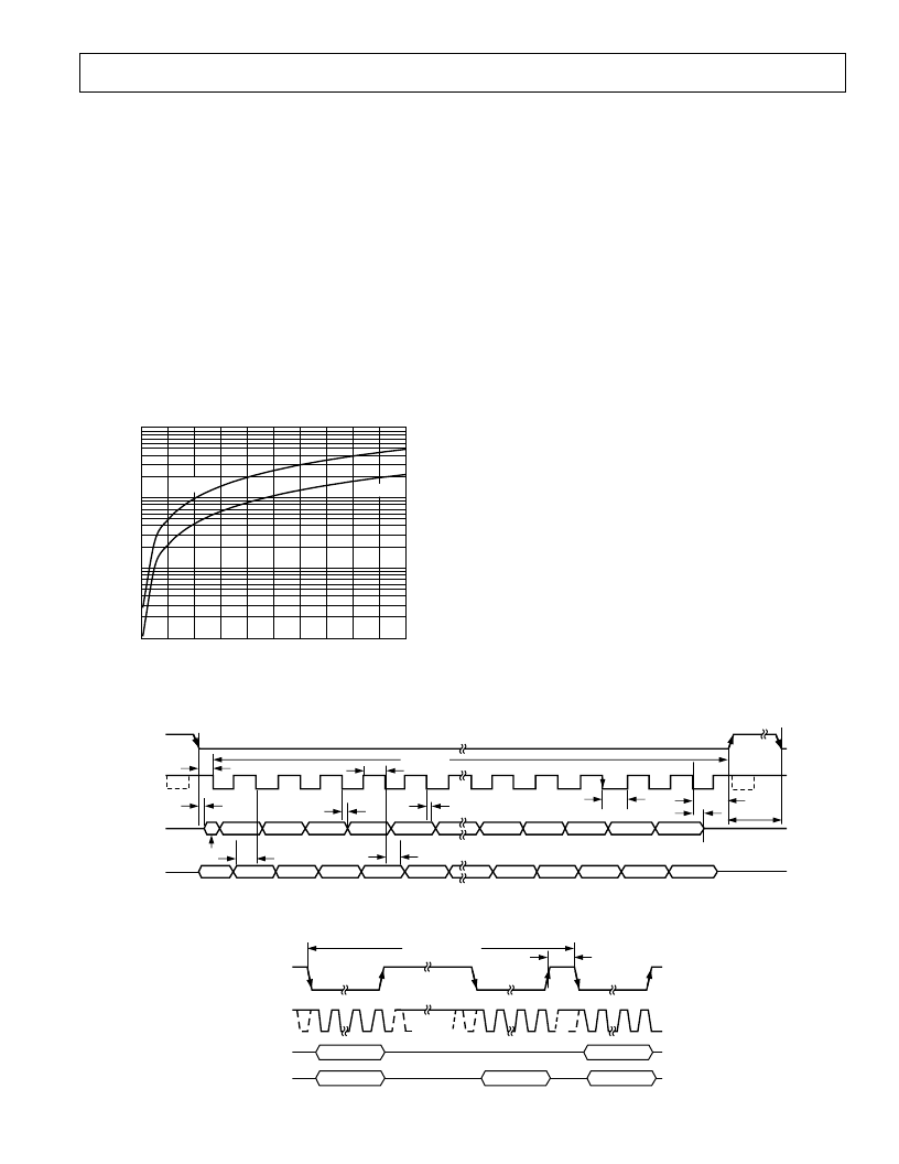
Figure 15 shows the maximum power versus throughput rate
when using the Auto Shutdown Mode with 5 V and 3 V supplies.
THROUGHPUT – kSPS
10
0
200
P
0.1
0.01
80
1
100
140
180
20
40
60
120
160
AV
DD
= 5V
AV
DD
= 3V
Figure 15. Power vs. Throughput Rate
SERIAL INTERFACE
Figures 16 shows the detailed timing diagrams for serial inter-
facing to the AD7923. The serial clock provides the conversion
clock and controls the transfer of information to and from the
AD7923 during each conversion.
The
CS
signal initiates the data transfer and conversion process.
The falling edge of
CS
puts the track-and-hold into hold mode,
takes the bus out of three-state, and the analog input is sampled
at this point. The conversion is also initiated at this point and
will require 16 SCLK cycles to complete. The track-and-hold
will go back into track on the 14th SCLK falling edge as shown
in Figure 16 at Point B. On the 16th SCLK falling edge the
DOUT line will go back into three-state. If the rising edge of
CS
occurs before 16 SCLKs have elapsed, the conversion will be
terminated and the DOUT line will go back into three-state and
the Control Register will not be updated; otherwise DOUT
returns to three-state on the 16th SCLK falling edge, as shown
in Figure 16.
Sixteen serial clock cycles are required to perform the conversion
process and to access data from the AD7923. For the AD7923,
the twelve bits of data are preceded by two leading zeros and
two channel address bits ADD1 and ADD0, identifying which
channel the result corresponds to.
CS
going low clocks out the
first leading zero to be read in by the microcontroller or DSP on
the first falling edge of SCLK. The first falling edge of SCLK
will also clock out the second leading zero to be read in by the
microcontroller or DSP on the second SCLK falling edge, and
so on. The remaining two address bits and 12-data bits are then
clocked out by subsequent SCLK falling edges beginning with
the first address bit ADD1, thus the second falling clock edge
on the serial clock has the second leading zero provided and also
clocks out address bit ADD1. The final bit in the data transfer is
valid on the 16th falling edge, having been clocked out on the
previous (15th) falling edge.
CS
SCLK
DOUT
DIN
t
2
t
3
t
9
SEQ1
t
4
t
7
t
5
t
11
t
8
t
QUIET
t
6
t
CONVERT
1
2
3
4
5
6
11
12
13
14
15
16
THREE-
STATE
ZERO
ADD1
2 IDENTIFICATION
BITS
ADD0
DB11
DB10
DB4
DB3
DB2
DB1
DB0
THREE-
STATE
t
10
ZERO
B
WRITE
DONTC
DONTC
ADD1
ADD0
CODING
DONTC
DONTC
DONTC
DONTC
Figure 16. Serial Interface Timing Diagram
CS
t
QUIET
MIN
t
CYCLE
5 s MIN
1
16
1
16
1
16
SCLK
VALID DATA
VALID DATA
DOUT
POWER-UP
DIN
Figure 17. General Timing Diagram
相關PDF資料 |
PDF描述 |
|---|---|
| AD7940BRJ-R2 | 3mW, 100kSPS, 14-Bit ADC in 6-Lead SOT-23 |
| AD7947 | 3mW, 100kSPS, 14-Bit ADC in 6-Lead SOT-23 |
| AD7940BRJ-REEL7 | 3mW, 100kSPS, 14-Bit ADC in 6-Lead SOT-23 |
| AD7680 | 3mW, 100kSPS, 14-Bit ADC in 6-Lead SOT-23 |
| AD7683 | 3mW, 100kSPS, 14-Bit ADC in 6-Lead SOT-23 |
相關代理商/技術參數(shù) |
參數(shù)描述 |
|---|---|
| AD7923BRU-REEL | 制造商:Analog Devices 功能描述:ADC Single SAR 200ksps 12-bit Serial 16-Pin TSSOP T/R 制造商:Analog Devices 功能描述:ADC SGL SAR 200KSPS 12-BIT SERL 16TSSOP - Tape and Reel |
| AD7923BRU-REEL7 | 制造商:Analog Devices 功能描述:ADC Single SAR 200ksps 12-bit Serial 16-Pin TSSOP T/R |
| AD7923BRUZ | 功能描述:IC ADC 12BIT 4CH W/SEQ 16TSSOP RoHS:是 類別:集成電路 (IC) >> 數(shù)據(jù)采集 - 模數(shù)轉(zhuǎn)換器 系列:- 標準包裝:1 系列:microPOWER™ 位數(shù):8 采樣率(每秒):1M 數(shù)據(jù)接口:串行,SPI? 轉(zhuǎn)換器數(shù)目:1 功率耗散(最大):- 電壓電源:模擬和數(shù)字 工作溫度:-40°C ~ 125°C 安裝類型:表面貼裝 封裝/外殼:24-VFQFN 裸露焊盤 供應商設備封裝:24-VQFN 裸露焊盤(4x4) 包裝:Digi-Reel® 輸入數(shù)目和類型:8 個單端,單極 產(chǎn)品目錄頁面:892 (CN2011-ZH PDF) 其它名稱:296-25851-6 |
| AD7923BRUZ-REEL | 功能描述:IC ADC 12BIT 4CH W/SEQ 16TSSOP RoHS:是 類別:集成電路 (IC) >> 數(shù)據(jù)采集 - 模數(shù)轉(zhuǎn)換器 系列:- 標準包裝:2,500 系列:- 位數(shù):16 采樣率(每秒):15 數(shù)據(jù)接口:MICROWIRE?,串行,SPI? 轉(zhuǎn)換器數(shù)目:1 功率耗散(最大):480µW 電壓電源:單電源 工作溫度:-40°C ~ 85°C 安裝類型:表面貼裝 封裝/外殼:38-WFQFN 裸露焊盤 供應商設備封裝:38-QFN(5x7) 包裝:帶卷 (TR) 輸入數(shù)目和類型:16 個單端,雙極;8 個差分,雙極 配用:DC1011A-C-ND - BOARD DELTA SIGMA ADC LTC2494 |
| AD7923BRUZ-REEL7 | 功能描述:IC ADC 12BIT 4CH W/SEQ 16TSSOP RoHS:是 類別:集成電路 (IC) >> 數(shù)據(jù)采集 - 模數(shù)轉(zhuǎn)換器 系列:- 標準包裝:1 系列:microPOWER™ 位數(shù):8 采樣率(每秒):1M 數(shù)據(jù)接口:串行,SPI? 轉(zhuǎn)換器數(shù)目:1 功率耗散(最大):- 電壓電源:模擬和數(shù)字 工作溫度:-40°C ~ 125°C 安裝類型:表面貼裝 封裝/外殼:24-VFQFN 裸露焊盤 供應商設備封裝:24-VQFN 裸露焊盤(4x4) 包裝:Digi-Reel® 輸入數(shù)目和類型:8 個單端,單極 產(chǎn)品目錄頁面:892 (CN2011-ZH PDF) 其它名稱:296-25851-6 |
發(fā)布緊急采購,3分鐘左右您將得到回復。