- 您現在的位置:買賣IC網 > PDF目錄373927 > AD7992 (Analog Devices, Inc.) 2-Channel, 12-Bit ADC with I2C Compatible Interface in 10-Lead MSOP PDF資料下載
參數資料
| 型號: | AD7992 |
| 廠商: | Analog Devices, Inc. |
| 英文描述: | 2-Channel, 12-Bit ADC with I2C Compatible Interface in 10-Lead MSOP |
| 中文描述: | 2通道,12位I2C兼容接口的ADC的10引腳MSOP |
| 文件頁數: | 6/21頁 |
| 文件大小: | 266K |
| 代理商: | AD7992 |
AD7992
–6–
REV. PrH
PRELIMINARY TECHNICAL DATA
PIN FUNCTION DESCRIPTION
Pin
Mnemonic
Function
AGND
Analog Ground. Ground reference point for all circuitry on the AD7992. All analog input
signals should be referred to this GND voltage.
Power Supply Input. The V
DD
range for the AD7992 is from +2.7V to +5.5V.
Analog Input 2 / Voltage Reference Input. In single-channel mode, this pin becomes the
reference voltage input, and an external reference should be applied at this pin. The external
reference input range is 1.2V to V
DD
. A 1 μF capacitor should be tied between this pin and
AGND. If bit D6 is set to 1 in the Configuration Register the AD7992 will operate in single
channel mode. In dual Channel mode, D6 in configuration register is 0, this pin provides the
second analog input channel. The reference voltage for the AD7992 is taken from the power
supply voltage in dual channel mode.
Analog Input 1. Single-ended analog input channel. The input range is 0V to REF
IN
.
Logic Input. Address Select input which selects one of three I
2
C addresses for the AD7992 as
shown in Table I.
Logic Input Signal. Convert Start Signal. This is an edge triggered logic input. The rising
edge of this signal powers up the part. The power up time for the part is 1
μ
s. The falling
edge of
CONVST
places the track/hold into hold mode and initiates a conversion. A power
up time of at least 1
μ
s must be allowed for the
CONVST
high pulse, otherwise the conver-
sion result will be invalid. (See Modes of Operation Section)
Digital Output, selectable as an ALERT or BUSY output function. When configured as an
ALERT output, this pin acts as an Out of Range Indicator, and if enabled it becomes active
when the conversion result violates the DATA
HIGH
or DATA
LOW
values. See Limit Registers
section. When configured as a BUSY output, this pin becomes active when a conversion is in
progress. Open-Drain Output. External pull-up resister required.
Digital I/O. Serial Bus Bi-directional Data. Open-drain output. External pull-up resistor
required.
Digital Input. Serial Bus Clock. Open Drain. External pull-up resistor required.
V
DD
V
IN
2/REF
IN
V
IN
1
AS
CONVST
ALERT/BUSY
SDA
SCL
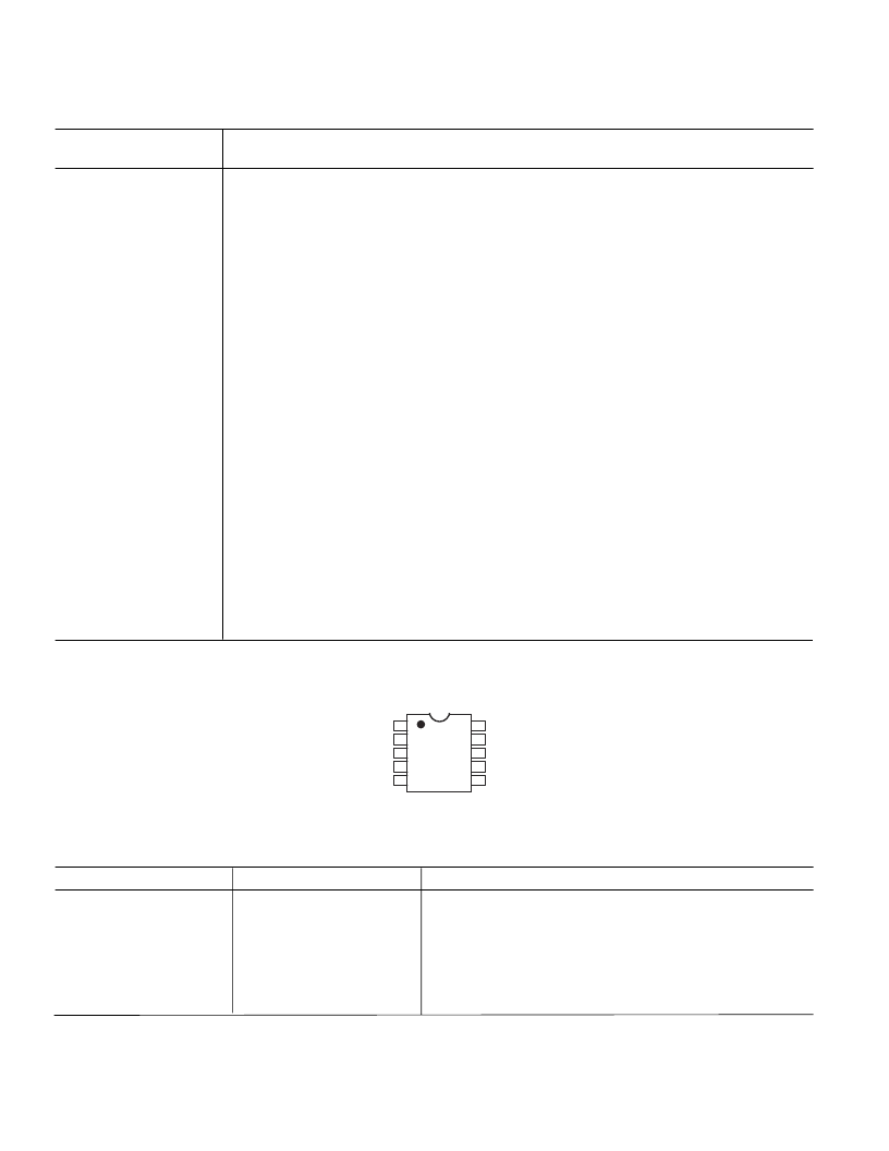
AD7992 PIN CONFIGURATION MSOP
Table I. I
2
C Address Selection
Part Number
AS Pin
I
2
C Address
AD7992-0
AD7992-0
AD7992-1
AD7992-1
GND
V
DD
GND
V
DD
010 0001
010 0010
010 0011
010 0100
AD7992-X
1
Float
010 0000
Note:-
1.
If the AS pin is left floating on any of the AD7992 parts the device address will be 010 0000. This will give each AD7992 device three differ-
ent address options.
AD7992
TOP VIEW
(Not to Scale)
1
2
3
4
7
8
9
10
SDA
SCL
VDD
AGND
VIN1
ALERT
6
5
AGND
VIN2 / REFIN
AS
相關PDF資料 |
PDF描述 |
|---|---|
| AD7992BRM-0 | 2-Channel, 12-Bit ADC with I2C Compatible Interface in 10-Lead MSOP |
| AD7992BRM-1 | 2-Channel, 12-Bit ADC with I2C Compatible Interface in 10-Lead MSOP |
| AD7994BRU-0 | 4-Channel, 12-/10-Bit ADCs with I2C Compatible Interface in 16-Lead TSSOP |
| AD7994BRU-1 | 4-Channel, 12-/10-Bit ADCs with I2C Compatible Interface in 16-Lead TSSOP |
| AD7993BRU-0 | 4-Channel, 12-/10-Bit ADCs with I2C Compatible Interface in 16-Lead TSSOP |
相關代理商/技術參數 |
參數描述 |
|---|---|
| AD7992_05 | 制造商:AD 制造商全稱:Analog Devices 功能描述:2-Channel, 12-Bit ADC with I2C-Compatible |
| AD7992BRM-0 | 制造商:Analog Devices 功能描述:ADC Single SAR 188ksps 12-bit Serial 10-Pin MSOP |
| AD7992BRM-0REEL | 制造商:Analog Devices 功能描述:ADC Single SAR 188ksps 12-bit Serial 10-Pin MSOP T/R |
| AD7992BRM-1 | 制造商:Analog Devices 功能描述:ADC Single SAR 188ksps 12-bit Serial 10-Pin MSOP 制造商:Rochester Electronics LLC 功能描述:2-CHANNEL, 12-BIT ADC WITH 12C ITF I.C. - Bulk |
| AD7992BRM-1REEL | 制造商:Analog Devices 功能描述:ADC Single SAR 188ksps 12-bit Serial 10-Pin MSOP T/R |
發布緊急采購,3分鐘左右您將得到回復。