- 您現在的位置:買賣IC網 > PDF目錄373928 > AD8009 (Analog Devices, Inc.) 1 GHz, 5,500 V/us Low Distortion Amplifier PDF資料下載
參數資料
| 型號: | AD8009 |
| 廠商: | Analog Devices, Inc. |
| 英文描述: | 1 GHz, 5,500 V/us Low Distortion Amplifier |
| 中文描述: | 1千兆赫,5,500 V的/我們的低失真放大器 |
| 文件頁數: | 9/12頁 |
| 文件大小: | 229K |
| 代理商: | AD8009 |
AD8009
–9–
REV. B
FREQUENCY
–
MHz
10
1000
100
G
–
8
7
6
5
4
–
1
3
2
1
0
12
9
6
3
0
–
15
–
12
–
9
–
6
–
3
G
–
50
V
IN
C
A
499
V
OUT
= 200mV p
–
p
V
OUT
499
100
C
A
= 0pF
1 dB/div
C
= 1pF
1 dB/div
C
A
= 2pF
3 dB/div
1
Figure 34. Small Signal Frequency Response vs. Parasitic
Capacitance
1.5ns
40mV
V
OUT
= 200mV p
–
p
V
S
= 5V
C
A
= 2pF
C
A
= 1pF
C
A
= 0pF
499
100
50
C
A
V
OUT
V
IN
499
Figure 35. Small Signal Pulse Response vs. Parasitic
Capacitance
10 F
AD8009
HP8753D
49.9
301
49.9
+5V
–
5V
301
2
10 F
+
Z
OUT
= 50
Z
IN
= 50
+
0.001 F
0.1 F
0.001 F
0.1 F
3
7
4
6
WAVETEK 5201
BPF
Figure 36. AD8009 Driving a Bandpass RF Filter
CENTER 50.000 MHz
SPAN 80.000 MHz
0
–
10
–
20
–
30
–
40
–
50
–
60
–
70
–
80
–
90
R
–
AD8009
G = 2
R
= R
G
= 301
DRIVING
WAVETEK 5201
TUNABLE BPF
f
C
= 50MHz
Figure 37. Frequency Response of Bandpass Filter Circuit
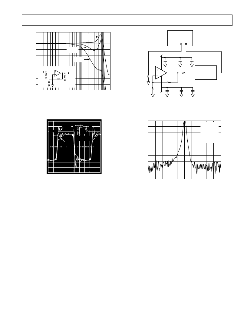
APPLICATIONS
All current feedback op amps are affected by stray capacitance
on their –INPUT. Figures 34 and 35 illustrate the AD8009’s
response to such capacitance.
Figure 34 shows the bandwidth can be extended by placing a
capacitor in parallel with the gain resistor. The small signal pulse
response corresponding to such an increase in capacitance/
bandwidth is shown in Figure 35.
As a practical consideration, the higher the capacitance on the
–INPUT to GND, the higher R
F
needs to be to minimize
peaking/ringing.
RF Filter Driver
The output drive capability, wide bandwidth and low distortion
of the AD8009 are well suited for creating gain blocks that can
drive RF filters. Many of these filters require that the input be
driven by a 50
source, while the output must be terminated in
50
for the filters to exhibit their specified frequency response.
Figure 36 shows a circuit for driving and measuring the
frequency response of a filter, a Wavetek 5201 Tunable Band
Pass Filter that is tuned to a 50 MHz center frequency. The
HP8753D network provides a stimulus signal for the measure-
ment. The analyzer has a 50
source impedance that drives a
cable that is terminated in 50
at the high impedance nonin-
verting input of the AD8009.
The AD8009 is set at a gain of two. The series 50
resistor at
the output, along with the 50
termination provided by the
filter and its termination, yield an overall unity gain for the
measured path. The frequency response plot of Figure 37
shows the circuit to have an insertion loss of 1.3 dB in the pass
band and about 75 dB rejection in the stop band.
相關PDF資料 |
PDF描述 |
|---|---|
| AD8009AR | 1 GHz, 5,500 V/us Low Distortion Amplifier |
| AD8009ART | 1 GHz, 5,500 V/us Low Distortion Amplifier |
| AD8009ART-REEL | 1 GHz, 5,500 V/us Low Distortion Amplifier |
| AD8009ART-REEL7 | Buffer with 3-State Output |
| AD8009AR-REEL | 1 GHz, 5,500 V/us Low Distortion Amplifier |
相關代理商/技術參數 |
參數描述 |
|---|---|
| AD8009_04 | 制造商:AD 制造商全稱:Analog Devices 功能描述:1 GHz, 5,500 V/Я Low Distortion Amplifier |
| AD80090BBCZ | 制造商:Analog Devices 功能描述: |
| AD80090BBCZRL | 制造商:Analog Devices 功能描述: |
| AD80098 | 制造商:Analog Devices 功能描述: |
| AD8009ACHIPS | 制造商:AD 制造商全稱:Analog Devices 功能描述:1 GHz, 5,500 V/Я Low Distortion Amplifier |
發布緊急采購,3分鐘左右您將得到回復。