- 您現在的位置:買賣IC網 > PDF目錄373929 > AD8019ARU-EVAL (Analog Devices, Inc.) DSL Line Driver with Power-Down PDF資料下載
參數資料
| 型號: | AD8019ARU-EVAL |
| 廠商: | Analog Devices, Inc. |
| 英文描述: | DSL Line Driver with Power-Down |
| 中文描述: | DSL線路驅動器,掉電 |
| 文件頁數: | 4/20頁 |
| 文件大小: | 782K |
| 代理商: | AD8019ARU-EVAL |
REV. 0
AD8019
–4–
CAUTION
ESD (electrostatic discharge) sensitive device. Electrostatic charges as high as 4000 V readily
accumulate on the human body and test equipment and can discharge without detection. Although
the AD8019 features proprietary ESD protection circuitry, permanent damage may occur on
devices subjected to high-energy electrostatic discharges. Therefore, proper ESD precautions are
recommended to avoid performance degradation or loss of functionality.
WARNING!
ESD SENSITIVE DEVICE
ABSOLUTE MAXIMUM RATINGS
1
Supply Voltage . . . . . . . . . . . . . . . . . . . . . . . . . . . . . . . . 26.4 V
Internal Power Dissipation
TSSOP-14 Package
2
. . . . . . . . . . . . . . . . . . . . . . . . . 2.2 W
SOIC-8 Package
3
. . . . . . . . . . . . . . . . . . . . . . . . . . . 1.4 W
Input Voltage (Common-Mode) . . . . . . . . . . . . . . . . . . . .
±
V
S
Differential Input Voltage . . . . . . . . . . . . . . . . . . . . . . . . .
±
V
S
Output Short Circuit Duration
. . . . . . . . . . . . . . . . . . . . Observe Power Derating Curves
Storage Temperature Range . . . . . . . . . . . . –65
°
C to +125
°
C
Operating Temperature Range . . . . . . . . . . . –40
°
C to +85
°
C
Lead Temperature Range (Soldering 10 sec) . . . . . . . . . 300
°
C
NOTES
1
Stresses above those listed under Absolute Maximum Ratings may cause perma-
nent damage to the device. This is a stress rating only; functional operation of the
device at these or any other conditions above those indicated in the operational
section of this specification is not implied. Exposure to absolute maximum rating
conditions for extended periods may affect device reliability.
2
Specification is for device on a four-layer board with 10 inches
2
of 1 oz. copper at
85
°
C 14-lead TSSOP package:
θ
= 90
°
C/W.
3
Specification is for device on a four-layer board with 10 inches
2
of 1 oz. copper at
85
°
C 8-lead SOIC package:
θ
JA
= 100
°
C/W.
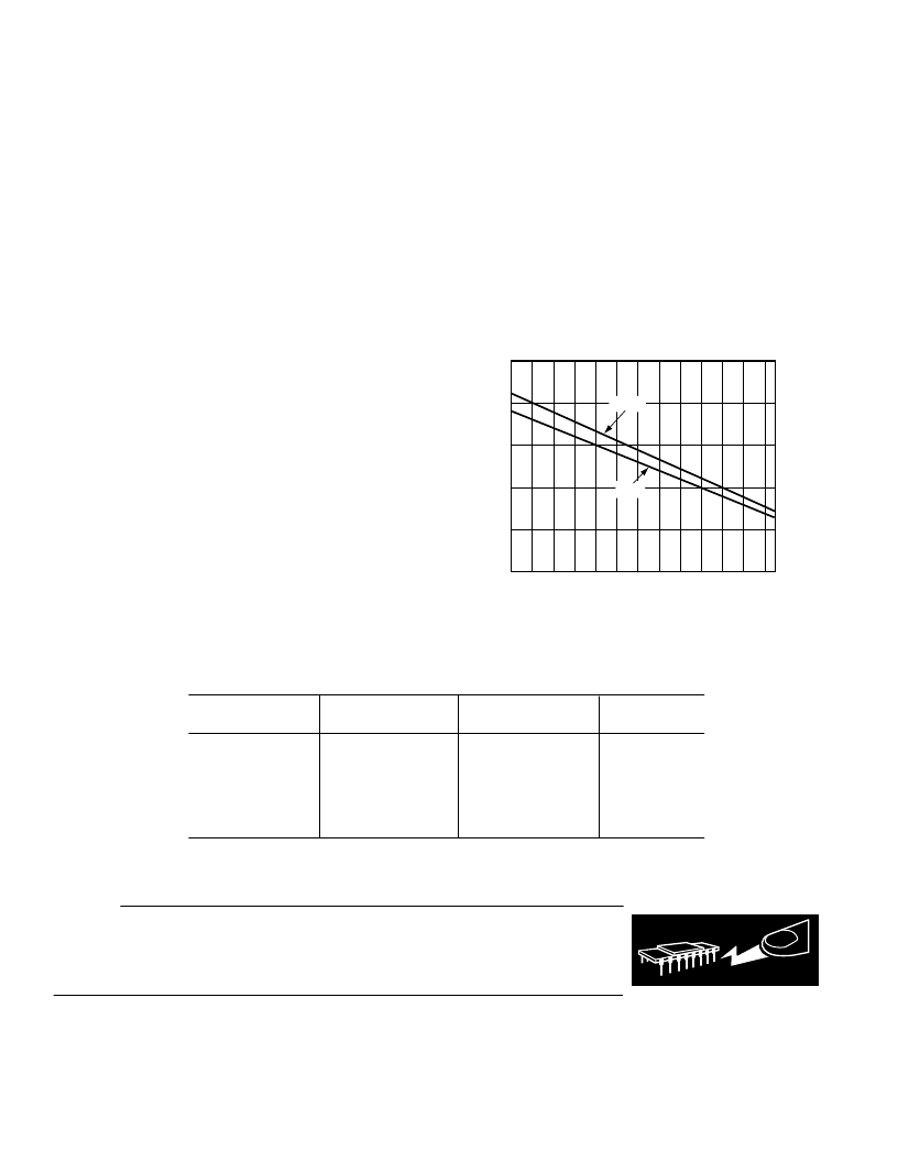
MAXIMUM POWER DISSIPATION
The maximum power that can be safely dissipated by the AD8019
is limited by the associated rise in junction temperature. The
maximum safe junction temperature for a plastic encapsulated
device is determined by the glass transition temperature of the
plastic, approximately 150
°
C. Temporarily exceeding this limit
may cause a shift in parametric performance due to a change in
the stresses exerted on the die by the package.
The output stage of the AD8019 is designed for maximum load
current capability. As a result, shorting the output to common
can cause the AD8019 to source or sink 500 mA. To ensure
proper operation, it is necessary to observe the maximum power
derating curves. Direct connection of the output to either power
supply rail can destroy the device.
AMBIENT TEMPERATURE
–
C
M
–
2.5
2.0
1.5
1.0
0.5
0
–
40
–
30
–
20
–
10
0
10
20
30
40
50
60
70
80
SOIC
TSSOP
Figure 2. Plot of Maximum Power Dissipation vs.
Temperature for AD8019 for T
J
= 150
°
C
ORDERING GUIDE
Temperature
Range
–40
°
C to +85
°
C
–40
°
C to +85
°
C
–40
°
C to +85
°
C
–40
°
C to +85
°
C
–40
°
C to +85
°
C
–40
°
C to +85
°
C
Package
Description
Package
Option
Model
AD8019ARU
AD8019ARU-Reel
AD8019ARU-EVAL
AD8019AR
AD8019AR-Reel
AD8019AR-EVAL
14-Lead TSSOP
14-Lead TSSOP
Evaluation Board
8-Lead SOIC
8-Lead SOIC
Evaluation Board
RU-14
RU-14 Reel
ARU-EVAL
R-8
R-8 Reel
AR EVAL
相關PDF資料 |
PDF描述 |
|---|---|
| AD8019ARU-REEL | DSL Line Driver with Power-Down |
| AD8019 | DSL Line Driver with Power-Down |
| AD8019AR | DSL Line Driver with Power-Down |
| AD8019ARU | DSL Line Driver with Power-Down |
| AD8019AR-EVAL | DSL Line Driver with Power-Down |
相關代理商/技術參數 |
參數描述 |
|---|---|
| AD8019ARU-REEL | 制造商:Analog Devices 功能描述:ADSL Driver Dual 180MHz 14-Pin TSSOP T/R 制造商:Analog Devices 功能描述:ADSL DRVR DUAL 180MHZ 14TSSOP - Tape and Reel 制造商:Rochester Electronics LLC 功能描述:TSSOP DSL LINE DRIVER WITH POWER DOWN - Tape and Reel |
| AD8019ARUZ | 制造商:Analog Devices 功能描述:ADSL Driver Dual 180MHz 14-Pin TSSOP |
| AD8019ARZ | 制造商:Analog Devices 功能描述:ADSL Driver Dual 180MHz 8-Pin SOIC N |
| AD802 | 制造商:未知廠家 制造商全稱:未知廠家 功能描述:AD800/AD802: Clock Recovery and Data Retiming Phase-Locked Loop Data Sheet (Rev. B. 12/93) |
發(fā)布緊急采購,3分鐘左右您將得到回復。