- 您現在的位置:買賣IC網 > PDF目錄373929 > AD8019ARU-REEL (ANALOG DEVICES INC) DSL Line Driver with Power-Down PDF資料下載
參數資料
| 型號: | AD8019ARU-REEL |
| 廠商: | ANALOG DEVICES INC |
| 元件分類: | 通用總線功能 |
| 英文描述: | DSL Line Driver with Power-Down |
| 中文描述: | DUAL LINE DRIVER, PDSO14 |
| 封裝: | TSSOP-14 |
| 文件頁數: | 11/20頁 |
| 文件大小: | 782K |
| 代理商: | AD8019ARU-REEL |
REV. 0
AD8019
–11–
R
L
–
V
S
+V
O
+V
S
–
V
O
+V
S
–
V
S
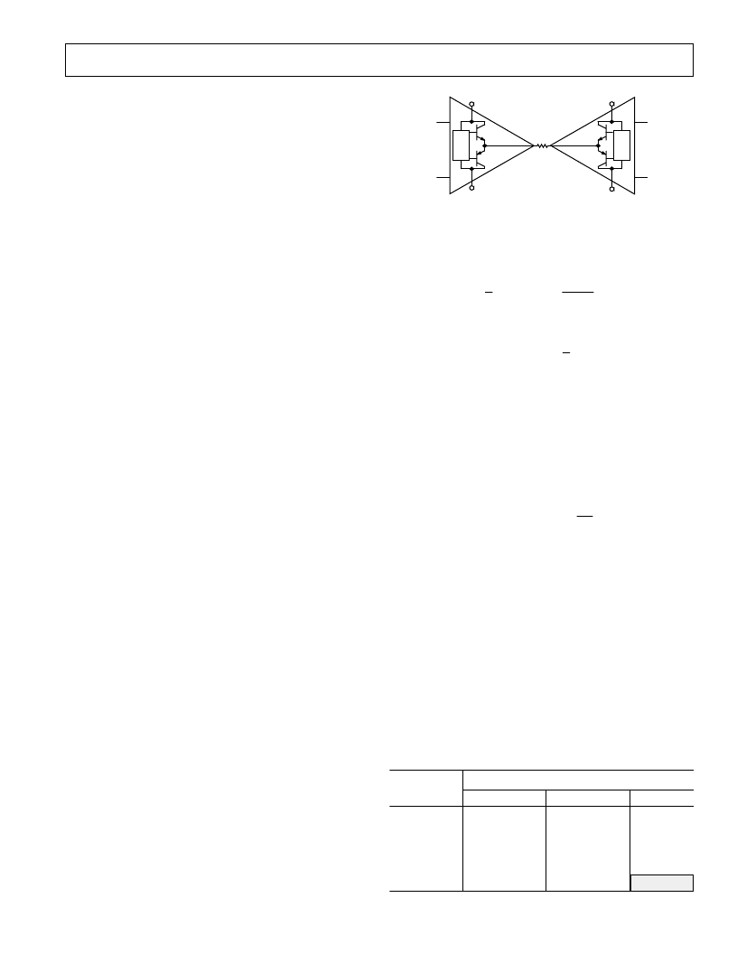
Figure 3. Simplified Differential Driver
Remembering that each output device only dissipates for half
the time gives a simple integral that computes the power for
each device:
1
2
2
∫
×
(
–
)
(
)
V
V
V
R
S
O
O
L
The total supply power can then be computed as:
P
V
(
V
V
I V
P
TOT
S
O
O
S
OUT
=
∫
∫
×
+
+
4
1
2
2
2
|
|
)
α
In this differential driver, V
O
is the voltage at the output of one
amplifier, so 2 V
O
is the voltage across R
L
. R
L
is the total
impedance seen by the differential driver, including back
termination
.
Now, with two observations the integrals are easily
evaluated. First, the integral of V
O2
is simply the square of the
rms value of V
O
. Second, the integral of | V
O
| is equal to the
average rectified value of V
O
, sometimes called the mean average
deviation, or MAD. It can be shown that for a DMT signal, the
MAD value is equal to 0.8 times the rms value.
P
V rmsV
V rms
R
I V
P
TOT
S
L
S
OUT
=
×
+
+
4 0 8
( .
1
2
2
–
)
α
For the AD8019 operating on a single 12 V supply and delivering a
total of 16 dBm (13 dBm to the line and 3 dBm to the matching
network) into 17.3
(100
reflected back through a 1:1.7
transformer plus back termination), the dissipated power is:
= 332
mW
+ 40
mW
= 372
mW
Using these calculations and a
θ
JA
of 90
°
C/W for the TSSOP
package and 100
°
C/W for the SOIC, Tables I
–
IV show junc-
tion temperature versus power delivered to the line for several
supply voltages while operating with an ambient temperature
of 85
°
C. The shaded areas indicate operation at a junction
temperature over the absolute maximum rating of 150
°
C, and
should be avoided.
Table I. Junction Temperature vs. Line Power and Operating
Voltage for TSSOP
V
SUPPLY
12
132
134
136
139
141
143
P
LINE
, dBm
13
14
15
16
17
18
12.5
134
137
139
141
144
147
13
137
139
141
144
147
150
GENERAL INFORMATION
The AD8019 is a voltage feedback amplifier with high output
current capability. As a voltage feedback amplifier, the AD8019
features lower current noise and more applications flexibility than
current feedback designs. It is fabricated on Analog Devices
’
proprietary High Voltage eXtra Fast Complementary Bipolar
Process (XFCB-HV), which enables the construction of PNP
and NPN transistors with similar f
T
s in the 4 GHz region. The
process is dielectrically isolated to eliminate the parasitic and
latch-up problems caused by junction isolation. These features
enable the construction of high-frequency, low-distortion amplifiers.
POWER-DOWN FEATURE
A digitally programmable logic pin (PWDN) is available on the
TSSOP-14 package. It allows the user to select between two
operating conditions, full on and shutdown. The DGND pin is
the logic reference. The threshold for the PWDN pin is typically
1.8 V above DGND. If the power-down feature is not being
used, it is better to tie the DGND pin to the lowest potential
that the AD8019 is tied to and place the PWDN pin at a poten-
tial at least 3 V higher than that of the DGND pin, but lower
than the positive supply voltage.
POWER SUPPLY AND DECOUPLING
The AD8019 can be powered with a good quality (i.e., low-noise)
supply anywhere in the range from +12 V to
±
12 V. In order to
optimize the ADSL upstream drive capability of 13 dBm and
maintain the best Spurious Free Dynamic Range (SFDR), the
AD8019 circuit should be powered with a well-regulated supply.
Careful attention must be paid to decoupling the power supply.
High quality capacitors with low equivalent series resistance
(ESR) such as multilayer ceramic capacitors (MLCCs) should
be used to minimize supply voltage ripple and power dissipa-
tion. In addition, 0.1
μ
F MLCC decoupling capacitors should
be located no more than 1/8 inch away from each of the power
supply pins. A large, usually tantalum, 10
μ
F to 47
μ
F capacitor
is required to provide good decoupling for lower frequency
signals and to supply current for fast, large signal changes at
the AD8019 outputs.
POWER DISSIPATION
It is important to consider the total power dissipation of the
AD8019 in order to properly size the heat sink area of an appli-
cation. Figure 3 is a simple representation of a differential driver.
With some simplifying assumptions we can estimate the total
power dissipated in this circuit. If the output current is large
compared to the quiescent current, computing the dissipation
in the output devices and adding it to the quiescent power dissipa-
tion will give a close approximation of the total power dissipation in
the package. A factor
α
(~0.6-1) corrects for the slight error
due to the Class A/B operation of the output stage. It can be
estimated by subtracting the quiescent current in the output
stage from the total quiescent current and ratioing that to the
total quiescent current. For the AD8019,
α
= 0.833.
相關PDF資料 |
PDF描述 |
|---|---|
| AD8019 | DSL Line Driver with Power-Down |
| AD8019AR | DSL Line Driver with Power-Down |
| AD8019ARU | DSL Line Driver with Power-Down |
| AD8019AR-EVAL | DSL Line Driver with Power-Down |
| AD8019AR-REEL | DSL Line Driver with Power-Down |
相關代理商/技術參數 |
參數描述 |
|---|---|
| AD8019ARUZ | 制造商:Analog Devices 功能描述:ADSL Driver Dual 180MHz 14-Pin TSSOP |
| AD8019ARZ | 制造商:Analog Devices 功能描述:ADSL Driver Dual 180MHz 8-Pin SOIC N |
| AD802 | 制造商:未知廠家 制造商全稱:未知廠家 功能描述:AD800/AD802: Clock Recovery and Data Retiming Phase-Locked Loop Data Sheet (Rev. B. 12/93) |
| AD80201Z | 制造商:Analog Devices 功能描述: |
發布緊急采購,3分鐘左右您將得到回復。