- 您現在的位置:買賣IC網 > PDF目錄373930 > AD8030 (Analog Devices, Inc.) Low Power, High Speed Rail-to-Rail Input/Output Amplifier PDF資料下載
參數資料
| 型號: | AD8030 |
| 廠商: | Analog Devices, Inc. |
| 英文描述: | Low Power, High Speed Rail-to-Rail Input/Output Amplifier |
| 中文描述: | 低功耗,高速軌到軌輸入/輸出放大器 |
| 文件頁數: | 16/20頁 |
| 文件大小: | 649K |
| 代理商: | AD8030 |
AD8029/AD8030/AD8040
APPLICATIONS
WIDEBAND OPERATION
Rev. A | Page 16 of 20
+V
S
–V
S
C2
10
μ
F
C1
0.1
μ
F
C4
0.1
μ
F
C3
10
μ
F
V
OUT
+
–
AD8029
R
G
R1
R
F
DISABLE
V
IN
R1 = R
F
||R
G
03679-0-052
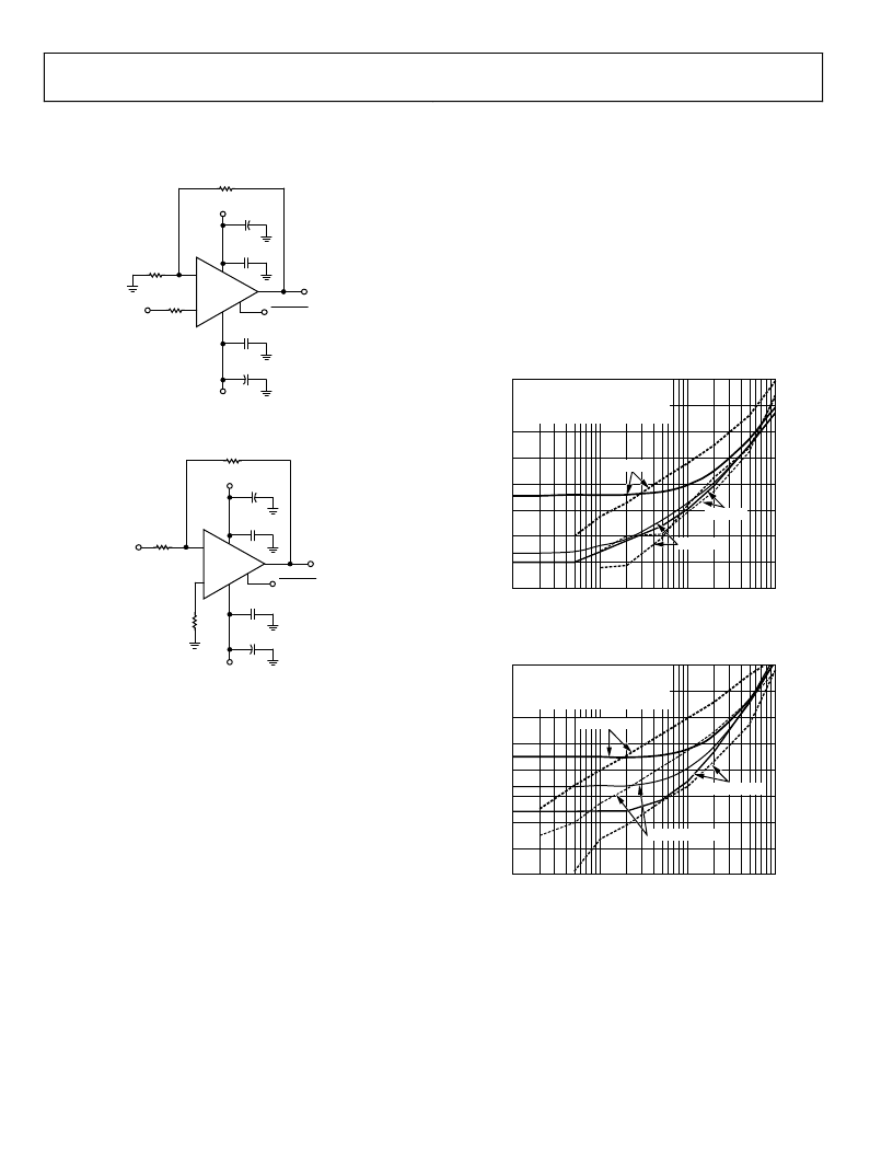
Figure 51. Wideband Non-inverting Gain Configuration
+V
S
–V
S
C1
0.1
μ
F
C4
0.1
μ
F
C3
10
μ
F
R1
V
OUT
–
AD8029
+
R
G
R1 = R
F
||R
G
R
F
V
IN
03679-0-053
C2
10
μ
F
DISABLE
Figure 52. Wideband Inverting Gain Configuration
OUTPUT LOADING SENSITIVITY
To achieve maximum performance and low power dissipation,
the designer needs to consider the loading at the output of
AD8029/AD8030/AD8040. Table 5 shows the effects of output
loading and performance.
When operating at unity gain, the effective load at the amplifier
output is the resistance (R
L
) being driven by the amplifier. For
gains other than 1, in noninverting configurations, the feedback
network represents an additional current load at the amplifier
output. The feedback network (R
F
+ R
G
) is in parallel with R
L
,
which lowers the effective resistance at the output of the
amplifier. The lower effective resistance causes the amplifier to
supply more current at the output. Lower values of feedback
resistance increase the current draw, thus increasing the
amplifier’s power dissipation.
For example, if using the values shown in Table 5 for a gain of 2,
with resistor values of 2.5 k, the effective load at the output is
1.67 k. For inverting configurations, only the feedback resistor
R
F
is in parallel with the output load. If the load is greater than
that specified in the data sheet, the amplifier can introduce
nonlinearities in its open-loop response, which increases
distortion. Figure 53 and Figure 54 illustrate effective output
loading and distortion performance. Increasing the resistance of
the feedback network can reduce the current consumption, but
has other implications.
FREQUENCY (MHz)
H
0.01
–120
0.1
1.0
10
0
–40
–50
–60
–70
–80
–90
–100
–110
= 0.1V p-p
V
= 2.0V p-p
SECOND HARMONIC – SOLID LINES
THIRD HARMONIC – DOTTED LINES
R
L
= 5k
R
L
= 2.5k
V
S
= 5V
R
L
= 1k
Figure 53. Gain of 1 Distortion
FREQUENCY (MHz)
H
0.01
–120
0.1
1.0
10
0
–40
–50
–60
–70
–80
–90
–100
–110
= 0.1V p-p
V
= 2.0V p-p
SECOND HARMONIC – SOLID LINES
THIRD HARMONIC – DOTTED LINES
R
F
= R
L
= 1k
V
S
= 5V
R
F
= R
L
= 5k
R
F
= R
L
= 2.5k
Figure 54. Gain of 2 Distortion
相關PDF資料 |
PDF描述 |
|---|---|
| AD8030AR | Low Power, High Speed Rail-to-Rail Input/Output Amplifier |
| AD8030AR-REEL | Low Power, High Speed Rail-to-Rail Input/Output Amplifier |
| AD8030AR-REEL7 | Low Power, High Speed Rail-to-Rail Input/Output Amplifier |
| AD8040 | Low Power, High Speed Rail-to-Rail Input/Output Amplifier |
| AD8040AR | Low Power, High Speed Rail-to-Rail Input/Output Amplifier |
相關代理商/技術參數 |
參數描述 |
|---|---|
| AD80305BBCZ | 制造商:Analog Devices 功能描述:- Rail/Tube |
| AD80305XBCZ | 制造商:Analog Devices 功能描述:X-GRADE VERSION OF AD80305BBCZ, CATALINA RFIC, 1X1, 144CSBGA - Rail/Tube |
| AD8030AR | 功能描述:IC AMP GP R-R DUAL LP 8SOIC RoHS:否 類別:集成電路 (IC) >> Linear - Amplifiers - Instrumentation 系列:- 標準包裝:100 系列:- 放大器類型:通用 電路數:1 輸出類型:- 轉換速率:0.2 V/µs 增益帶寬積:- -3db帶寬:- 電流 - 輸入偏壓:100pA 電壓 - 輸入偏移:30µV 電流 - 電源:380µA 電流 - 輸出 / 通道:- 電壓 - 電源,單路/雙路(±):±2 V ~ 18 V 工作溫度:0°C ~ 70°C 安裝類型:表面貼裝 封裝/外殼:8-SOIC(0.154",3.90mm 寬) 供應商設備封裝:8-SO 包裝:管件 |
| AD8030AR | 制造商:Analog Devices 功能描述:AMP LOW POWER RRI/O 8030 SOIC8 |
| AD8030AR-EBZ | 功能描述:BOARD EVAL FOR AD8030AR RoHS:是 類別:編程器,開發系統 >> 評估板 - 運算放大器 系列:- 產品培訓模塊:Lead (SnPb) Finish for COTS Obsolescence Mitigation Program 標準包裝:1 系列:- |
發布緊急采購,3分鐘左右您將得到回復。