- 您現(xiàn)在的位置:買賣IC網(wǎng) > PDF目錄373930 > AD8030 (Analog Devices, Inc.) Low Power, High Speed Rail-to-Rail Input/Output Amplifier PDF資料下載
參數(shù)資料
| 型號: | AD8030 |
| 廠商: | Analog Devices, Inc. |
| 英文描述: | Low Power, High Speed Rail-to-Rail Input/Output Amplifier |
| 中文描述: | 低功耗,高速軌到軌輸入/輸出放大器 |
| 文件頁數(shù): | 17/20頁 |
| 文件大小: | 649K |
| 代理商: | AD8030 |
AD8029/AD8030/AD8040
Table 5. Effect of Load on Performance
Noninverting
Gain
(k)
1
0
1
0
1
0
2
1
2
2.5
2
5
–1
1
–1
2.5
–1
5
Rev. A | Page 17 of 20
R
F
R
G
(k)
N/A
N/A
N/A
1
2.5
5
1
2.5
5
R
LOAD
(k)
1
2
5
1
2.5
5
1
2.5
5
–3 dB SS BW
(MHz)
120
130
139
36
44.5
43
40
40
34
Peaking
(dB)
0.02
0.6
1
0
0.2
2
0.01
0.05
1
HD2 at 1 MHz,
2 V p-p (dB)
–80
–84
–87.5
–72
–79
–84
–68
–74
–78
HD3 at 1 MHz,
2 V p-p (dB)
–72
–83
–92.5
–60
–72.5
–86
–57
–68
–80
Output Noise
(nV/√Hz)
16.5
16.5
16.5
33.5
34.4
36
33.6
34
36
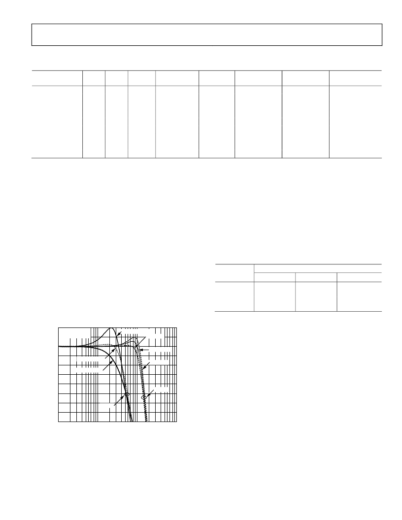
The feedback resistance (R
F
|| R
G
) combines with the input
capacitance to form a pole in the amplifier’s loop response. This
can cause peaking and ringing in the amplifier’s response if the
RC time constant is too low. Figure 55 illustrates this effect.
Peaking can be reduced by adding a small capacitor (1 pF–4 pF)
across the feedback resistor. The best way to find the optimal
value of capacitor is to empirically try it in your circuit. Another
factor of higher resistance values is the impact it has on noise
performance. Higher resistor values generate more noise. Each
application is unique and therefore a balance must be reached
between distortion, peaking, and noise performance. Table 5
outlines the trade-offs that different loads have on distortion,
peaking, and noise performance. In gains of 1, 2, and 10,
equivalent loads of 1 k, 2 k, and 5 k are shown.
With increasing load resistance, the distortion and –3 dB
bandwidth improve, while the noise and peaking degrade
slightly.
R
L
= 5k
FREQUENCY (MHz)
N
1
–8
10
100
1000
0
2
1
0
–1
–2
–3
–4
–5
–6
R
L
= 2.5k
–7
R
F
= R
L
= 5k
R
F
= R
L
= 2.5k
R
F
= R
L
= 1k
G = +2
G = +1
R
L
= 1k
V
S
= 5V
V
OUT
= 0.1V p-p
Figure 55. Frequency Response for Various Feedback/Load Resistances
DISABLE PIN
The AD8029 disable pin allows the amplifier to be shut down
for power conservation or multiplexing applications. When in
the disable mode, the amplifier draws only 150 μA of quiescent
current. The disable pin control voltage is referenced to the
negative supply. The amplifier enters power-down mode any
time the disable pin is tied to the most negative supply or within
0.8 V of the negative supply. If left open, the amplifier will
operate normally. For switching levels, refer to Table 6.
Table 6. Disable Pin Control Voltage
Disable Pin
Voltage
+3 V
Low
(Disabled)
0 V to <0.8 V
High
(Enabled)
1.2 V to 3 V
Supply Voltage
+5 V
±
5 V
0 V to <0.8 V
–5 V to <–4 .2 V
1.2 V to 5 V
–3.8 V to +5 V
相關(guān)PDF資料 |
PDF描述 |
|---|---|
| AD8030AR | Low Power, High Speed Rail-to-Rail Input/Output Amplifier |
| AD8030AR-REEL | Low Power, High Speed Rail-to-Rail Input/Output Amplifier |
| AD8030AR-REEL7 | Low Power, High Speed Rail-to-Rail Input/Output Amplifier |
| AD8040 | Low Power, High Speed Rail-to-Rail Input/Output Amplifier |
| AD8040AR | Low Power, High Speed Rail-to-Rail Input/Output Amplifier |
相關(guān)代理商/技術(shù)參數(shù) |
參數(shù)描述 |
|---|---|
| AD80305BBCZ | 制造商:Analog Devices 功能描述:- Rail/Tube |
| AD80305XBCZ | 制造商:Analog Devices 功能描述:X-GRADE VERSION OF AD80305BBCZ, CATALINA RFIC, 1X1, 144CSBGA - Rail/Tube |
| AD8030AR | 功能描述:IC AMP GP R-R DUAL LP 8SOIC RoHS:否 類別:集成電路 (IC) >> Linear - Amplifiers - Instrumentation 系列:- 標(biāo)準(zhǔn)包裝:100 系列:- 放大器類型:通用 電路數(shù):1 輸出類型:- 轉(zhuǎn)換速率:0.2 V/µs 增益帶寬積:- -3db帶寬:- 電流 - 輸入偏壓:100pA 電壓 - 輸入偏移:30µV 電流 - 電源:380µA 電流 - 輸出 / 通道:- 電壓 - 電源,單路/雙路(±):±2 V ~ 18 V 工作溫度:0°C ~ 70°C 安裝類型:表面貼裝 封裝/外殼:8-SOIC(0.154",3.90mm 寬) 供應(yīng)商設(shè)備封裝:8-SO 包裝:管件 |
| AD8030AR | 制造商:Analog Devices 功能描述:AMP LOW POWER RRI/O 8030 SOIC8 |
| AD8030AR-EBZ | 功能描述:BOARD EVAL FOR AD8030AR RoHS:是 類別:編程器,開發(fā)系統(tǒng) >> 評估板 - 運算放大器 系列:- 產(chǎn)品培訓(xùn)模塊:Lead (SnPb) Finish for COTS Obsolescence Mitigation Program 標(biāo)準(zhǔn)包裝:1 系列:- |
發(fā)布緊急采購,3分鐘左右您將得到回復(fù)。