- 您現在的位置:買賣IC網 > PDF目錄373930 > AD8030 (Analog Devices, Inc.) Low Power, High Speed Rail-to-Rail Input/Output Amplifier PDF資料下載
參數資料
| 型號: | AD8030 |
| 廠商: | Analog Devices, Inc. |
| 英文描述: | Low Power, High Speed Rail-to-Rail Input/Output Amplifier |
| 中文描述: | 低功耗,高速軌到軌輸入/輸出放大器 |
| 文件頁數: | 6/20頁 |
| 文件大小: | 649K |
| 代理商: | AD8030 |
AD8029/AD8030/AD8040
ABSOLUTE MAXIMUM RATINGS
Table 4. AD8029/AD8030/AD8040 Stress Ratings
Parameter
Supply Voltage
Power Dissipation
Common-Mode Input Voltage
Differential Input Voltage
Storage Temperature
Operating Temperature Range
Lead Temperature Range
(Soldering 10 sec)
Junction Temperature
Rev. A | Page 6 of 20
Rating
12.6 V
See Figure 6
±V
S
± 0.5 V
±1.8 V
–65°C to +125°C
–40°C to +125°C
300°C
150°C
Stresses above those listed under Absolute Maximum Ratings
may cause permanent damage to the device. This is a stress
rating only; functional operation of the device at these or any
other conditions above those indicated in the operational
section of this specification is not implied. Exposure to absolute
maximum rating conditions for extended periods may affect
device reliability.
MAXIMUM POWER DISSIPATION
The maximum safe power dissipation in the AD8029/AD8030/
AD8040 package is limited by the associated rise in junction
temperature (T
J
) on the die. The plastic encapsulating the die
locally reaches the junction temperature. At approximately
150°C, which is the glass transition temperature, the plastic
changes its properties. Even temporarily exceeding this
temperature limit may change the stresses that the package
exerts on the die, permanently shifting the parametric
performance of the AD8029/AD8030/AD8040. Exceeding a
junction temperature of 175°C for an extended period can
result in changes in silicon devices, potentially causing failure.
The still-air thermal properties of the package and PCB (θ
JA
),
ambient temperature (
T
A
), and the total power dissipated in the
package (
P
D
) determine the junction temperature of the die. The
junction temperature can be calculated as
T
J
=
T
A
+ (
P
D
×
θ
JA
)
The power dissipated in the package (
P
D
) is the sum of the
quiescent power dissipation and the power dissipated in the
package due to the load drive for all outputs. The quiescent
power is the voltage between the supply pins (
V
S
) times the
quiescent current (
I
S
). Assuming the load (
R
L
) is referenced to
midsupply, the total drive power is
V
S
/2 × I
OUT
, some of which is
dissipated in the package and some in the load (V
OUT
× I
OUT
).
The difference between the total drive power and the load
power is the drive power dissipated in the package.
P
D
=
Quiescent Power
+ (
Total Drive Power
–
Load Power
)
(
)
L
OUT
R
L
OUT
R
S
S
S
D
V
V
V
I
V
P
2
–
2
×
+
×
=
RMS output voltages should be considered. If
R
L
is referenced to
V
S
–, as in single-supply operation, then the total drive power is
V
S
× I
OUT
.
If the rms signal levels are indeterminate, consider the worst
case, when
V
OUT
=
V
S
/4 for
R
L
to midsupply:
(
)
(
)
L
S
R
S
S
D
V
I
V
P
2
4
+
×
=
In single-supply operation with
R
L
referenced to
V
S
–, worst case
is
V
OUT
=
V
S
/2.
Airflow will increase heat dissipation, effectively reducing θ
JA
.
Also, more metal directly in contact with the package leads
from metal traces, through holes, ground, and power planes will
reduce the θ
JA
. Care must be taken to minimize parasitic capaci-
tances at the input leads of high speed op amps, as discussed in
the PCB Layout section.
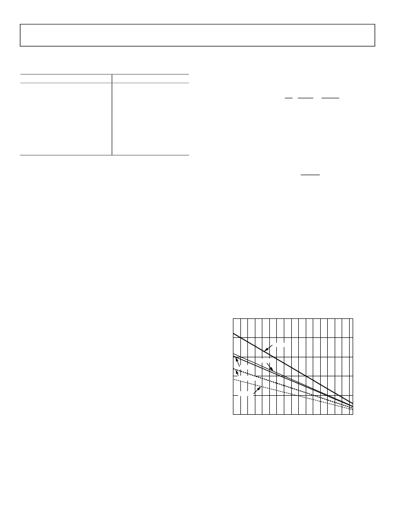
Figure 6 shows the maximum safe power dissipation in the
package versus the ambient temperature for the SOIC-8
(125°C/W), SOT23-8 (160°C/W), SOIC-14 (90°C/W),
TSSOP-14 (120°C/W), and SC70-6 (208°C/W) packages on a
JEDEC standard 4-layer board. θ
JA
values are approximations.
–40
–20–10
–30
0
10 20 30 40 50 60 70 80 90 100110120
AMBIENT TEMPERATURE (°C)
2.5
M
1.0
0.5
1.5
2.0
0
SOIC-8
TSSOP-14
SOIC-14
SOT-23-8
SC70-6
0
Figure 6. Maximum Power Dissipation
Output Short Circuit
Shorting the output to ground or drawing excessive current
from the AD8029/AD8030/AD8040 could cause catastrophic
failure.
相關PDF資料 |
PDF描述 |
|---|---|
| AD8030AR | Low Power, High Speed Rail-to-Rail Input/Output Amplifier |
| AD8030AR-REEL | Low Power, High Speed Rail-to-Rail Input/Output Amplifier |
| AD8030AR-REEL7 | Low Power, High Speed Rail-to-Rail Input/Output Amplifier |
| AD8040 | Low Power, High Speed Rail-to-Rail Input/Output Amplifier |
| AD8040AR | Low Power, High Speed Rail-to-Rail Input/Output Amplifier |
相關代理商/技術參數 |
參數描述 |
|---|---|
| AD80305BBCZ | 制造商:Analog Devices 功能描述:- Rail/Tube |
| AD80305XBCZ | 制造商:Analog Devices 功能描述:X-GRADE VERSION OF AD80305BBCZ, CATALINA RFIC, 1X1, 144CSBGA - Rail/Tube |
| AD8030AR | 功能描述:IC AMP GP R-R DUAL LP 8SOIC RoHS:否 類別:集成電路 (IC) >> Linear - Amplifiers - Instrumentation 系列:- 標準包裝:100 系列:- 放大器類型:通用 電路數:1 輸出類型:- 轉換速率:0.2 V/µs 增益帶寬積:- -3db帶寬:- 電流 - 輸入偏壓:100pA 電壓 - 輸入偏移:30µV 電流 - 電源:380µA 電流 - 輸出 / 通道:- 電壓 - 電源,單路/雙路(±):±2 V ~ 18 V 工作溫度:0°C ~ 70°C 安裝類型:表面貼裝 封裝/外殼:8-SOIC(0.154",3.90mm 寬) 供應商設備封裝:8-SO 包裝:管件 |
| AD8030AR | 制造商:Analog Devices 功能描述:AMP LOW POWER RRI/O 8030 SOIC8 |
| AD8030AR-EBZ | 功能描述:BOARD EVAL FOR AD8030AR RoHS:是 類別:編程器,開發系統 >> 評估板 - 運算放大器 系列:- 產品培訓模塊:Lead (SnPb) Finish for COTS Obsolescence Mitigation Program 標準包裝:1 系列:- |
發布緊急采購,3分鐘左右您將得到回復。