- 您現在的位置:買賣IC網 > PDF目錄373933 > AD8055 (Analog Devices, Inc.) Voltage Feedback Amplifiers(低成本,電壓反饋放大器) PDF資料下載
參數資料
| 型號: | AD8055 |
| 廠商: | Analog Devices, Inc. |
| 英文描述: | Voltage Feedback Amplifiers(低成本,電壓反饋放大器) |
| 中文描述: | 電壓反饋放大器(低成本,電壓反饋放大器) |
| 文件頁數: | 9/12頁 |
| 文件大小: | 230K |
| 代理商: | AD8055 |
AD8055/AD8056
–9–
REV. 0
APPLICATIONS
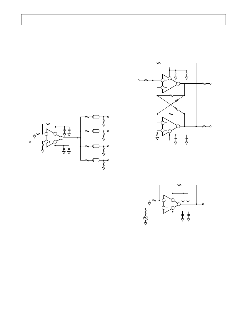
Four-Line Video Driver
The AD8055 is a useful low cost circuit for driving up to four
video lines. For such an application, the amplifier is configured
for a noninverting gain of 2 as shown in Figure 33. The input
video source is terminated in 75
and applied to the high
impedance noninverting input.
Each output cable is connected to the op amp output via a 75
series back termination resistor for proper cable termination.
The terminating resistors at the other ends of the lines will
divide the output signal by two, which is compensated for by
the gain-of-two of the op amp stage.
For a single load, the differential gain error of this circuit was
measured to be 0.01%, with a differential phase error of
0.02 degrees. The two load measurements were 0.02% and
0.03 degrees, respectively. For four loads, the differential gain
error is 0.02%, while the differential phase increases to 0.1
degrees.
0.1μF
10μF
75
402
AD8055
75
+5V
–5V
0.1μF
10μF
402
75
75
75
V
IN
75
75
75
75
V
OUT1
V
OUT2
V
OUT3
V
OUT4
6
7
2
3
4
Figure 33. Four-Line Video Driver
Single-Ended to Differential Line Driver
Creating differential signals from single-ended signals is
required for driving balanced, twisted pair cables, differential
input A/D converters and other applications that require differen-
tial signals. This is sometimes accomplished by using an inverting
and a noninverting amplifier stage to create the complementary
signals.
The circuit shown in Figure 34 shows how an AD8056 can be
used to make a single-ended to differential converter that offers
some advantages over the architecture mentioned above. Each
op amp is configured for unity gain by the feedback resistors
from the outputs to the inverting inputs. In addition, each out-
put drives the opposite op amp with a gain of –1 by means of the
crossed resistors. The result of this is that the outputs are comple-
mentary and there is high gain in the overall configuration.
Feedback techniques similar to a conventional op amp are used
to control the gain of the circuit. From the noninverting input
of Amp 1 to the output of Amp 2, is an inverting gain. Between
these points a feedback resistor can be used to close the loop.
As in the case of a conventional op amp inverting gain stage, an
input resistor is added to vary the gain.
The gain of this circuit from the input to Amp 1 output is R
F
/R
I
,
while the gain to the output of Amp 2 is –R
F
/R
I
. The circuit
thus creates a balanced differential output signal from a single-
ended input. The advantage of this circuit is that the gain can be
changed by changing a single resistor and still maintain the
balanced differential outputs.
75
R
I
402
+5V
R
F
402
–5V
AD8056
402
402
402
49.9
49.9
V
IN
+V
OUT
402
–V
OUT
10μF
0.1μF
1
2
3
8
AMP1
5
6
7
4
AMP2
10μF
0.1μF
Figure 34. Single-Ended to Differential Line Driver
Low Noise, Low Power Preamp
The AD8055 makes a good low cost, low noise, low power
preamp. A gain of 10 preamp can be made with a feedback
resistor of 909 ohms and a gain resistor of 100 ohms as shown in
Figure 35. The circuit has a –3 dB bandwidth of 20 MHz.
0.1μF
10μF
+5V
–5V
0.1μF
10μF
909
V
OUT
+
100
R
S
AD8055
6
7
2
3
4
Figure 35. Low Noise, Low Power Preamp with G = 10
and BW = 20 MHz
With a low source resistance (<approximately 100
), the major
contributors to the input referred noise of this circuit are the
input voltage noise of the amplifier and the noise of the 100
resistor. These are 6 nV
√
Hz
and 1.2 nV
√
Hz
, respectively.
These values yield a total input referred noise of 6.1 nV
√
Hz
.
相關PDF資料 |
PDF描述 |
|---|---|
| AD8056 | Voltage Feedback Amplifiers(低成本,電壓反饋放大器) |
| AD8056ARMZ-REEL7 | Low Cost, 300 MHz Voltage Feedback Amplifiers |
| AD8055ANZ | Low Cost, 300 MHz Voltage Feedback Amplifiers |
| AD8055ART-R2 | Low Cost, 300 MHz Voltage Feedback Amplifiers |
| AD8055ARTZ-R2 | Low Cost, 300 MHz Voltage Feedback Amplifiers |
相關代理商/技術參數 |
參數描述 |
|---|---|
| AD8055_06 | 制造商:AD 制造商全稱:Analog Devices 功能描述:Low Cost, 300 MHz Voltage Feedback Amplifiers |
| AD8055AN | 制造商:Analog Devices 功能描述:OP Amp Single Volt Fdbk 制造商:Rochester Electronics LLC 功能描述:PDIP HI IOUT, VLTG FDBK, LO COST OP AMP - Bulk 制造商:Analog Devices 功能描述:IC AMP HIGH SPEED 8055 DIP8 |
| AD8055ANZ | 功能描述:IC OPAMP VF LDIST LN LP 8DIP RoHS:是 類別:集成電路 (IC) >> Linear - Amplifiers - Instrumentation 系列:- 標準包裝:1 系列:- 放大器類型:通用 電路數:4 輸出類型:滿擺幅 轉換速率:0.028 V/µs 增益帶寬積:105kHz -3db帶寬:- 電流 - 輸入偏壓:3nA 電壓 - 輸入偏移:100µV 電流 - 電源:3.3µA 電流 - 輸出 / 通道:12mA 電壓 - 電源,單路/雙路(±):2.7 V ~ 12 V,±1.35 V ~ 6 V 工作溫度:-40°C ~ 85°C 安裝類型:表面貼裝 封裝/外殼:14-TSSOP(0.173",4.40mm 寬) 供應商設備封裝:14-TSSOP 包裝:剪切帶 (CT) 其它名稱:OP481GRUZ-REELCT |
| AD8055AR | 功能描述:IC OPAMP VF LDIST LN LP 8SOIC RoHS:否 類別:集成電路 (IC) >> Linear - Amplifiers - Instrumentation 系列:- 標準包裝:1,000 系列:- 放大器類型:電壓反饋 電路數:4 輸出類型:滿擺幅 轉換速率:33 V/µs 增益帶寬積:20MHz -3db帶寬:30MHz 電流 - 輸入偏壓:2nA 電壓 - 輸入偏移:3000µV 電流 - 電源:2.5mA 電流 - 輸出 / 通道:30mA 電壓 - 電源,單路/雙路(±):4.5 V ~ 16.5 V,±2.25 V ~ 8.25 V 工作溫度:-40°C ~ 85°C 安裝類型:表面貼裝 封裝/外殼:14-SOIC(0.154",3.90mm 寬) 供應商設備封裝:14-SOIC 包裝:帶卷 (TR) |
| AD8055AR-EBZ | 功能描述:BOARD EVAL FOR AD8055AR RoHS:是 類別:編程器,開發系統 >> 評估板 - 運算放大器 系列:- 產品培訓模塊:Lead (SnPb) Finish for COTS Obsolescence Mitigation Program 標準包裝:1 系列:- |
發布緊急采購,3分鐘左右您將得到回復。