- 您現在的位置:買賣IC網 > PDF目錄373937 > AD8123ACPZ-RL (ANALOG DEVICES INC) Triple Differential Receiver with Adjustable Line Equalization PDF資料下載
參數資料
| 型號: | AD8123ACPZ-RL |
| 廠商: | ANALOG DEVICES INC |
| 元件分類: | 通用總線功能 |
| 英文描述: | Triple Differential Receiver with Adjustable Line Equalization |
| 中文描述: | LINE RECEIVER, QCC40 |
| 封裝: | 6 X 6MM, ROHS COMPLIANT, MO-220VJJD-2, LFCSP-40 |
| 文件頁數: | 12/16頁 |
| 文件大小: | 618K |
| 代理商: | AD8123ACPZ-RL |
AD8123
SYNC PULSE EXTRACTION USING COMPARATORS
The AD8123 is useful in many systems that transport computer
video signals, which are typically comprised of red, green, and
blue (RGB) video signals and separate horizontal and vertical
sync signals. Because the sync signals are separate and not
embedded in the color signals, it is advantageous to transmit
them using a simple scheme that encodes them among the three
common-mode voltages of the RGB signals. The
AD8134
,
AD8147
, and
AD8148
triple differential drivers are natural
complements to the AD8123 seeing that they perform the sync
pulse encoding with the necessary circuitry on-chip.
The sync encoding equations follow:
[
H
V
V
Red
CM
2
[
V
2
2
[
H
V
V
Blue
CM
2
where:
Red V
CM
,
Green V
CM
, and
Blue V
CM
are the transmitted common-
mode voltages of the respective color signals.
K
is an adjustable gain constant that is set by the driver.
V
and
H
are the vertical and horizontal sync pulses, defined
with a weight of 1 when the pulses are in their low states, and a
weight of +1 when they are in their high states.
The
AD8134
and
AD8146/AD8147/AD8148
data sheets contain
further details regarding the encoding scheme. Figure 20 illustrates
how the AD8123 comparators can be used to extract the horizontal
and vertical sync pulses that are encoded on the RGB common-
mode voltages by the aforementioned drivers.
USING THE V
PEAK
, V
POLE
, V
GAIN
, AND V
OFFSET
INPUTS
The V
PEAK
input is the main peaking control and is used to
compensate for the low-pass roll-off in the cable response. The
V
POLE
input is a secondary frequency response shaping control
that shifts the positions of the equalizer poles. The V
GAIN
input
controls the wideband flat gain and is used to compensate for
the low frequency cable loss that is nominally flat. The V
OFFSET
input is used to produce an offset at the AD8123 output. The
output offset is equal to the voltage applied to the V
OFFSET
input,
limited by the output swing limits.
The V
PEAK
and V
POLE
controls can be used independently or they
can be coupled together to form a single peaking control. While
Figure 17 and Figure 18 show recommended settings vs. cable
length, designers may find other combinations that they prefer.
These two controls give designers extra freedom, as well as the
ability to compensate for different cable types (such as UTP and
coaxial cable), as opposed to having only a single frequency
shaping control.
Rev. 0 | Page 12 of 16
K
=
]
(1)
=
K
V
Green
CM
]
(2)
K
+
=
]
(3)
In some cases, as would likely be with automatic control, the
V
PEAK
control is derived from a low impedance source, such as
an op amp. Figure 21 shows how to derive V
POLE
from V
PEAK
in a
UTP application according to the recommended curves shown
in Figure 17, when V
PEAK
originates from a low impedance
source. Clearly, the 5 V supply must be clean to provide a clean
V
POLE
voltage.
0
V
PEAK
2
+ 0.9V
20
5.11k
V
PEAK
V
POLE
≈
5V
14k
8.25k
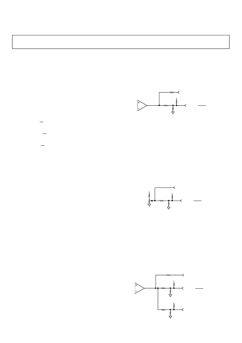
V
PEAK
Figure 21. Deriving V
POLE
from V
PEAK
with Low-Z Source for UTP Cable
The 20 Ω series resistor in the V
PEAK
path provides capacitive
load buffering for the op amp. This value can be modified,
depending on the actual capacitive load.
In automatic equalization circuits that place the control voltages
inside feedback loops, attention must be paid to the poles
produced by the summing resistors and load capacitances.
The peaking can also be adjusted by a mechanical or digitally
controlled potentiometer. In these cases, if the resistance of the
potentiometer is a couple of orders of magnitude lower than the
values of the resistors used to develop V
POLE
, its resistance can be
ignored. Figure 22 shows how to use a 500 Ω potentiometer with
the resistor values shown in Figure 21 scaled up by a factor of 10.
0
V
PEAK
2
+ 0.9V
51.1k
V
PEAK
V
POLE
≈
5V
5V
140k
82.5k
750
500
Figure 22. Deriving V
POLE
from V
PEAK
with Potentiometer for UTP Cable
Many potentiometers have wide tolerances. If a wide tolerance
potentiometer is used, it may be necessary to change the value
of the 750 Ω resistor to obtain a full swing for V
PEAK
.
The V
GAIN
input is essentially a contrast control and can be set
by adjusting it to produce the correct amplitude of a known test
signal (such as a white screen) at the AD8123 output.
V
GAIN
can also be derived from V
PEAK
according to the linear
relationships shown in Figure 17
and Figure 18. Figure 23 shows
how to derive V
POLE
and V
GAIN
from V
PEAK
in a UTP application
that originates from a low-Z source.
0
V
PEAK
2
+ 0.9V
20
5.11k
V
PEAK
V
POLE
≈
5V
14k
8.25k
5.11k
V
GAIN
≈
0.89 × V
PEAK
+ 0.38V
5V
60.4k
133k
V
PEAK
Figure 23. Deriving V
POLE
and V
GAIN
from V
PEAK
with Low-Z Source for UTP Cable
相關PDF資料 |
PDF描述 |
|---|---|
| AD8129AR | Low-Cost 270 MHz Differential Receiver Amplifiers |
| AD8129ARM | Low-Cost 270 MHz Differential Receiver Amplifiers |
| AD8129ARM-REEL3 | Low-Cost 270 MHz Differential Receiver Amplifiers |
| AD8129ARM-REEL72 | Low-Cost 270 MHz Differential Receiver Amplifiers |
| AD8130 | Low-Cost 270 MHz Differential Receiver Amplifiers |
相關代理商/技術參數 |
參數描述 |
|---|---|
| AD8123ACPZ-RL1 | 制造商:AD 制造商全稱:Analog Devices 功能描述:Triple Differential Receiver with Adjustable Line Equalization |
| AD8123ACPZ-TR | 制造商:Analog Devices 功能描述:TRIPLE EQUALIZER - Tape and Reel |
| AD8124 | 制造商:AD 制造商全稱:Analog Devices 功能描述:Triple Differential Receiver with 200 Meter Adjustable Cable Equalization |
| AD8124ACPZ | 功能描述:IC HS RCVR EQUALIZER 40VFQFN RoHS:是 類別:集成電路 (IC) >> 接口 - 驅動器,接收器,收發器 系列:- 標準包裝:250 系列:- 類型:收發器 驅動器/接收器數:2/2 規程:RS232 電源電壓:3 V ~ 5.5 V 安裝類型:表面貼裝 封裝/外殼:16-TSSOP(0.173",4.40mm 寬) 供應商設備封裝:16-TSSOP 包裝:帶卷 (TR) |
| AD8124ACPZ-R7 | 功能描述:IC RCVR TRPL DIFF EQUAL 40LFCSP RoHS:是 類別:集成電路 (IC) >> 接口 - 驅動器,接收器,收發器 系列:- 標準包裝:250 系列:- 類型:收發器 驅動器/接收器數:2/2 規程:RS232 電源電壓:3 V ~ 5.5 V 安裝類型:表面貼裝 封裝/外殼:16-TSSOP(0.173",4.40mm 寬) 供應商設備封裝:16-TSSOP 包裝:帶卷 (TR) |
發布緊急采購,3分鐘左右您將得到回復。