- 您現在的位置:買賣IC網 > PDF目錄373939 > AD8150-EVAL (Analog Devices, Inc.) 33 x 17, 1.5 Gbps Digital Crosspoint Switch PDF資料下載
參數資料
| 型號: | AD8150-EVAL |
| 廠商: | Analog Devices, Inc. |
| 英文描述: | 33 x 17, 1.5 Gbps Digital Crosspoint Switch |
| 中文描述: | 33 × 17,1.5 Gbps的數字交叉點開關 |
| 文件頁數: | 18/35頁 |
| 文件大小: | 995K |
| 代理商: | AD8150-EVAL |
第1頁第2頁第3頁第4頁第5頁第6頁第7頁第8頁第9頁第10頁第11頁第12頁第13頁第14頁第15頁第16頁第17頁當前第18頁第19頁第20頁第21頁第22頁第23頁第24頁第25頁第26頁第27頁第28頁第29頁第30頁第31頁第32頁第33頁第34頁第35頁
AD8150
–18–
REV. 0
V
CC
V
EE
DISABLE
I
OUT
OUTyyP
OUTyyN
V
CC
–
2V
V
EE
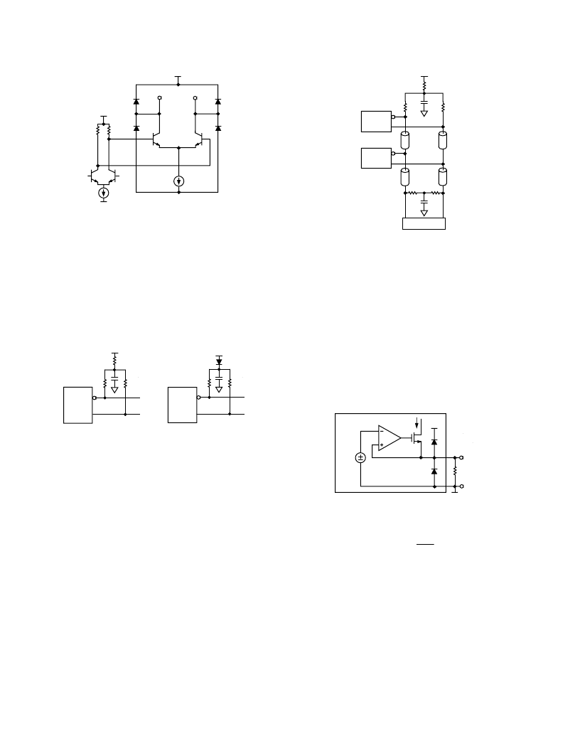
Figure 33. Simplified Output Circuit
To ensure proper operation, all outputs (including unused output)
must be pulled high using external pull-up networks to a level
within the output compliance range. If outputs from multiple
AD8150s are wired together, a single pull-up network may be
used for each output bus. The pull-up network should be chosen
to keep the output voltage levels within the output compliance
range at all times. Recommended pull-up networks to produce
PECL/ECL 100K and 10K compatible outputs are shown in
Figure 34. Alternatively, a separate supply can be used to pro-
vide V
COM
; making R
COM
and D
COM
unnecessary.
V
CC
R
COM
V
COM
R
L
OUTyyN
OUTyyP
AD8150
V
CC
D
COM
V
COM
R
L
OUTyyN
OUTyyP
AD8150
R
L
R
L
Figure 34. Output Pull-Up Networks: a) ECL 100K,
b) ECL 10K
The output levels are simply:
V
OH
=
V
COM
V
OL
=
V
COM
– I
OUT
R
L
V
SWING
= V
OH
– V
OL
= I
OUT
R
L
V
COM
=
V
CC
– I
OUT
R
COM
(
100K Mode
)
V
COM
=
V
CC
– V
(
D
COM
)
(
10K Mode
)
The common-mode adjustment element (R
COM
or D
COM
) may
be omitted if the input range of the receiver includes the positive
supply voltage. The bypass capacitors reduce common-mode
perturbations by providing an ac short from the common nodes
(V
COM
) to ground.
When busing together the outputs of multiple AD8150s or when
running at high data rates, double termination of its outputs is
recommended to mitigate the impact of reflections due to open
transmission line stubs and the lumped capacitance of the
AD8150 output pins. A possible connection is shown in Figure
35; the bypass capacitors provide an ac short from the common
nodes of the termination resistors to ground. To maintain signal
fidelity at high data rates, the stubs connecting the output pins
to the output transmission lines or load resistors should be as
short as possible.
V
CC
OUTyyN
OUTyyP
OUTyyN
OUTyyP
R
L
R
L
Z
O
Z
O
Z
O
Z
O
R
L
R
L
AD8150
AD8150
V
COM
R
COM
RECEIVER
Figure 35. Double Termination of AD8150 Outputs
In this case, the output levels are:
V
OH
=
V
COM
–
(1/4)
I
OUT
R
L
V
OL
=
V
COM
–
(3/4)
I
OUT
R
L
V
SWING
=
V
OH
–
V
OL
= (1/2)
I
OUT
R
L
Output Current Set Pin (REF)
A simplified schematic of the reference circuit is shown in Fig-
ure 36. A single external resistor connected between the REF
pin and V
EE
determines the output current for all output stages.
This feature allows a choice of pull-up networks and transmission
line characteristic impedances while still achieving a nominal
output swing of 800 mV. At low data rates, substantial power
savings can be achieved by using lower output swings and higher
load resistances.
AD8150
V
EE
R
SET
REF
V
CC
I
OUT
/25
1.25V
Figure 36. Simplified Reference Circuit
The resistor value current is given by the following expression:
R
I
SET
OUT
=
25
Example:
R
SET
= 1.54
k
for
I
OUT
= 16.2
mA
The minimum set resistor is R
SET,min
= 1 k
resulting in I
OUT,max
=
25 mA. The maximum set resistor is R
SET,max
= 5 k
result-
ing in I
OUT,min
= 5 mA. Nominal 800 mV output swings can be
achieved in a 50
load using R
SET
= 1.56 k
(I
OUT
= 16.2 mA)
or in a doubly-terminated 75
load using R
SET
= 1.17 k
(I
OUT
= 21.3 mA).
To minimize stray capacitance and avoid the pickup of unwanted
signals, the external set resistor should be located close to the
REF pin. Bypassing the set resistor is not recommended.
相關PDF資料 |
PDF描述 |
|---|---|
| AD8150 | 33 x 17, 1.5 Gbps Digital Crosspoint Switch |
| AD8150AST | 33 x 17, 1.5 Gbps Digital Crosspoint Switch |
| AD8151-EVAL | GPA/SK 300X280X1,5... |
| AD8151 | 33 x 17, 3.2 Gb/s Digital Crosspoint Switch |
| AD8151AST | 33 x 17, 3.2 Gb/s Digital Crosspoint Switch |
相關代理商/技術參數 |
參數描述 |
|---|---|
| AD8151 | 制造商:AD 制造商全稱:Analog Devices 功能描述:33 x 17, 3.2 Gb/s Digital Crosspoint Switch |
| AD8151AST | 制造商:AD 制造商全稱:Analog Devices 功能描述:33 x 17, 3.2 Gb/s Digital Crosspoint Switch |
| AD8151ASTZ | 功能描述:IC CROSSPOINT SWIT 33X17 184LQFP RoHS:是 類別:集成電路 (IC) >> 接口 - 模擬開關,多路復用器,多路分解器 系列:XStream™ 其它有關文件:STG4159 View All Specifications 標準包裝:5,000 系列:- 功能:開關 電路:1 x SPDT 導通狀態電阻:300 毫歐 電壓電源:雙電源 電壓 - 電源,單路/雙路(±):±1.65 V ~ 4.8 V 電流 - 電源:50nA 工作溫度:-40°C ~ 85°C 安裝類型:表面貼裝 封裝/外殼:7-WFBGA,FCBGA 供應商設備封裝:7-覆晶 包裝:帶卷 (TR) |
| AD8151-EVAL | 制造商:Analog Devices 功能描述:EVAL KIT FOR 33 17, 3.2 GBPS DGTL CROSSPOINT SWIT - Bulk |
| AD8151XSTZ | 功能描述:IC CROSSPOINT SWITCH 制造商:analog devices inc. 系列:* 零件狀態:上次購買時間 標準包裝:1 |
發布緊急采購,3分鐘左右您將得到回復。