- 您現(xiàn)在的位置:買賣IC網(wǎng) > PDF目錄373939 > AD815 (Analog Devices, Inc.) High Output Current Differential Driver(高輸出電流差分驅(qū)動器) PDF資料下載
參數(shù)資料
| 型號: | AD815 |
| 廠商: | Analog Devices, Inc. |
| 英文描述: | High Output Current Differential Driver(高輸出電流差分驅(qū)動器) |
| 中文描述: | 高輸出電流差動驅(qū)動器(高輸出電流差分驅(qū)動器) |
| 文件頁數(shù): | 11/16頁 |
| 文件大小: | 320K |
| 代理商: | AD815 |
AD815
REV. A
–11–
DC E RRORS AND NOISE
T here are three major noise and offset terms to consider in a
current feedback amplifier. For offset errors refer to the
equation below. For noise error the terms are root-sum-squared
to give a net output error. In the circuit below (Figure 42), they
are input offset (V
IO
) which appears at the output multiplied by
the noise gain of the circuit (1 + R
F
/R
G
), noninverting input
current (I
BN
×
R
N
) also multiplied by the noise gain, and the
inverting input current, which when divided between R
F
and R
G
and subsequently multiplied by the noise gain always appear at
the output as I
BI
×
R
F
. T he input voltage noise of the AD815 is
less than 2 nV/
√
Hz
. At low gains though, the inverting input
current noise times R
F
is the dominant noise source. Careful
layout and device matching contribute to better offset and drift
specifica-tions for the AD815 compared to many other current
feedback amplifiers. T he typical performance curves in
conjunction with the equations below can be used to predict the
performance of the AD815 in any application.
V
OUT
=
V
IO
×
1
+
R
F
R
G
±
I
BN
×
R
N
×
1
+
R
F
R
G
±
I
BI
×
R
F
I
BI
I
BN
R
G
R
N
R
F
V
OUT
Figure 42. Output Offset Voltage
POWE R CONSIDE RAT IONS
T he 500 mA drive capability of the AD815 enables it to drive a
50
load at 40 V p-p when it is configured as a differential
driver. T his implies a power dissipation, P
IN
, of nearly 5 watts.
T o ensure reliability, the junction temperature of the AD815
should be maintained at less than 175
°
C. For this reason, the
AD815 will require some form of heat sinking in most applica-
tions. T he thermal diagram of Figure 43 gives the basic
relationship between junction temperature (T
J
) and various
components of
θ
JA
.
T
J
=
T
A
+
P
IN
θ
J A
Equation 1
θ
A
(JUNCTION TO
DIE MOUNT)
θ
B
(DIE MOUNT
TO CASE)
θ
A
+
θ
B
=
θ
JC
CASE
T
A
T
J
θ
JC
θ
CA
T
A
θ
JA
T
J
P
IN
WHERE:
P
IN
= DEVICE DISSIPATION
T
A
= AMBIENT TEMPERATURE
T
J
= JUNCTION TEMPERATURE
θ
JC
= THERMAL RESISTANCE – JUNCTION TO CASE
θ
CA
= THERMAL RESISTANCE – CASE TO AMBIENT
Figure 43. A Breakdown of Various Package Thermal
Resistances
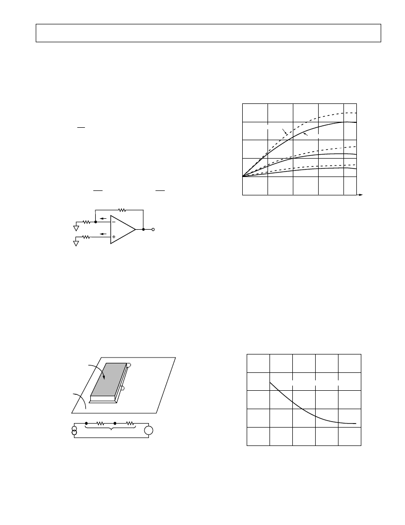
Figure 44 gives the relationship between output voltage swing
into various loads and the power dissipated by the AD815 (P
IN
).
T his data is given for both sine wave and square wave (worst
case) conditions. It should be noted that these graphs are for
mostly resistive (phase <
±
10
°
) loads. When the power dissipation
requirements are known, Equation 1 and the graph on Figure 45
can be used to choose an appropriate heat sinking configuration.
4
3
P
I
10
20
V
OUT
– Volts p-p
30
40
2
1
R
L
= 50
R
L
= 100
R
L
= 200
f = 1kHz
SQUARE WAVE
SINE WAVE
Figure 44. Total Power Dissipation vs. Differential Output
Voltage
Normally, the AD815 will be soldered directly to a copper pad.
Figure 45 plots
θ
JA
against size of copper pad. T his data pertains
to copper pads on both sides of G10 epoxy glass board connected
together with a grid of feedthroughs on 5 mm centers.
T his data shows that loads of 100 ohms or less will usually not
require any more than this. T his is a feature of the AD815’s 15-
lead power SIP package.
An important component of
θ
JA
is the thermal resistance of the
package to heatsink. T he data given is for a direct soldered
connection of package to copper pad. T he use of heatsink
grease either with or without an insulating washer will increase
this number. Several options now exist for dry thermal connec-
tions. T hese are available from Bergquist as part # SP600-90.
Consult with the manufacturer of these products for details of
their application.
COPPER HEAT SINK AREA (TOP AND BOTTOM) – mm
2
35
30
10
0
2.5k
0.5k
θ
J
°
C
1k
1.5k
2k
25
20
15
AD815AVR, AY
(θ
JC
= 2
°
C/W)
Figure 45. Power Package Thermal Resistance vs. Heat
Sink Area
相關(guān)PDF資料 |
PDF描述 |
|---|---|
| AD816 | 500 mA Differential Driver & Dual Low Noise (VF) Amplifiers(500mA差分驅(qū)動器和雙低噪電壓反饋放大器) |
| AD8170AN | 250 MHz, 10 ns Switching Multiplexers w/Amplifier |
| AD8170AR | 250 MHz, 10 ns Switching Multiplexers w/Amplifier |
| AD8170-EB | 250 MHz, 10 ns Switching Multiplexers w/Amplifier |
| AD8170AR-REEL | 250 MHz, 10 ns Switching Multiplexers w/Amplifier |
相關(guān)代理商/技術(shù)參數(shù) |
參數(shù)描述 |
|---|---|
| AD815_05 | 制造商:AD 制造商全稱:Analog Devices 功能描述:High Output Current Differential Driver |
| AD8150 | 制造商:AD 制造商全稱:Analog Devices 功能描述:33 x 17, 1.5 Gbps Digital Crosspoint Switch |
| AD8150AST | 制造商:Rochester Electronics LLC 功能描述:LQFP 1.5GBPS 33X17 DIGITAL CROSSPOINT SW - Tape and Reel 制造商:Analog Devices 功能描述:IC SWITCH CROSSPOINT |
| AD8150ASTZ | 功能描述:IC CROSSPOINT SWIT 33X17 184LQFP RoHS:是 類別:集成電路 (IC) >> 接口 - 模擬開關(guān),多路復(fù)用器,多路分解器 系列:XStream™ 應(yīng)用說明:Ultrasound Imaging Systems Application Note 產(chǎn)品培訓(xùn)模塊:Lead (SnPb) Finish for COTS Obsolescence Mitigation Program 標(biāo)準(zhǔn)包裝:250 系列:- 功能:開關(guān) 電路:單刀單擲 導(dǎo)通狀態(tài)電阻:48 歐姆 電壓電源:單電源 電壓 - 電源,單路/雙路(±):2.7 V ~ 5.5 V 電流 - 電源:5µA 工作溫度:0°C ~ 70°C 安裝類型:表面貼裝 封裝/外殼:48-LQFP 供應(yīng)商設(shè)備封裝:48-LQFP(7x7) 包裝:托盤 |
| AD8150ASTZ | 制造商:Analog Devices 功能描述:IC DIGITAL CROSSPOINT SWITCH |
發(fā)布緊急采購,3分鐘左右您將得到回復(fù)。