- 您現(xiàn)在的位置:買賣IC網(wǎng) > PDF目錄373939 > AD815 (Analog Devices, Inc.) High Output Current Differential Driver(高輸出電流差分驅(qū)動(dòng)器) PDF資料下載
參數(shù)資料
| 型號(hào): | AD815 |
| 廠商: | Analog Devices, Inc. |
| 英文描述: | High Output Current Differential Driver(高輸出電流差分驅(qū)動(dòng)器) |
| 中文描述: | 高輸出電流差動(dòng)驅(qū)動(dòng)器(高輸出電流差分驅(qū)動(dòng)器) |
| 文件頁(yè)數(shù): | 3/16頁(yè) |
| 文件大小: | 320K |
| 代理商: | AD815 |
第1頁(yè)第2頁(yè)當(dāng)前第3頁(yè)第4頁(yè)第5頁(yè)第6頁(yè)第7頁(yè)第8頁(yè)第9頁(yè)第10頁(yè)第11頁(yè)第12頁(yè)第13頁(yè)第14頁(yè)第15頁(yè)第16頁(yè)
AD815
REV. A
–3–
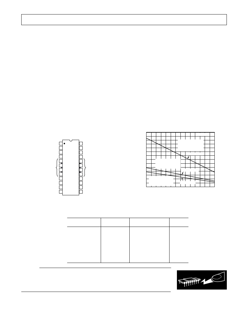
MAX IMUM POWE R DISSIPAT ION
T he maximum power that can be safely dissipated by the
AD815 is limited by the associated rise in junction temperature.
T he maximum safe junction temperature for the plastic encap-
sulated parts is determined by the glass transition temperature
of the plastic, about 150
°
C. Exceeding this limit temporarily
may cause a shift in parametric performance due to a change in
the stresses exerted on the die by the package. Exceeding a
junction temperature of 175
°
C for an extended period can result
in device failure.
T he AD815 has thermal shutdown protection, which guarantees
that the maximum junction temperature of the die remains below a
safe level, even when the output is shorted to ground. Shorting
the output to either power supply will result in device failure.
T o ensure proper operation, it is important to observe the
derating curves and refer to the section on power considerations.
It must also be noted that in high (noninverting) gain configura-
tions (with low values of gain resistor), a high level of input
overdrive can result in a large input error current, which may
result in a significant power dissipation in the input stage. T his
power must be included when computing the junction tempera-
ture rise due to total internal power.
AMBIENT TEMPERATURE –
°
C
14
7
4
–50
90
–40
M
–30 –20 –10
10
20 30
40
50 60
70 80
13
12
8
6
5
11
9
10
0
T
J
= 150
°
C
3
2
1
0
AD815 AVR, AY
θ
JA
= 41
°
C/W
(STILL AIR = 0FT/MIN)
NO HEAT SINK
θ
JA
= 52
°
C/W
(STILL AIR = 0 FT/MIN)
NO HEAT SINK
AD815ARB-24
θ
= 16
°
C/W
SOLDERED DOWN TO
COPPER HEAT SINK
(STILL AIR = 0FT/MIN)
AD815 AVR, AY
Plot of Maximum Power Dissipation vs. Temperature
ABSOLUT E MAX IMUM RAT INGS
1
Supply Voltage . . . . . . . . . . . . . . . . . . . . . . . . . . .
±
18 V T otal
Internal Power Dissipation
2
Plastic (Y & VR) . . . 3.05 Watts (Observe Derating Curves)
Small Outline (RB) . . 2.4 Watts (Observe Derating Curves)
Input Voltage (Common Mode) . . . . . . . . . . . . . . . . . . .
±
V
S
Differential Input Voltage . . . . . . . . . . . . . . . . . . . . . . . .
±
6 V
Output Short Circuit Duration
. . . . . . . . . . . . . . . . . . . . . . Observe Power Derating Curves
Can Only Short to Ground
Storage T emperature Range
Y, VR & RB Package . . . . . . . . . . . . . . . . –65
°
C to +125
°
C
Operating T emperature Range
AD815A . . . . . . . . . . . . . . . . . . . . . . . . . . . –40
°
C to +85
°
C
Lead T emperature Range (Soldering, 10 seconds) . . . . +300
°
C
NOT ES
1
Stresses above those listed under “Absolute Maximum Ratings” may cause
permanent damage to the device. T his is a stress rating only and functional
operation of the device at these or any other conditions above those indicated in the
operational section of this specification is not implied. Exposure to absolute
maximum rating conditions for extended periods may affect device reliability.
2
Specification is for device in free air with 0 ft/min air flow: 15-Pin T hrough Hole
and Surface Mount:
θ
JA
= 41
°
C/Watt; 24-Pin Surface Mount:
θ
JA
= 52
°
C/Watt.
PIN CONFIGURAT ION
24-Pin T hermally-E nhanced SOIC (RB-24)
TOP VIEW
(Not to Scale)
AD815
13
16
15
14
24
23
22
21
20
19
18
17
12
11
10
9
8
1
2
3
4
7
6
5
NC = NO CONNECT
NC
NC
NC
NC
NC
NC
NC
NC
+IN1
–IN1
–IN2
+IN2
OUT1
–V
S
OUT2
+V
S
*HEAT TABS ARE CONNECTED TO THE POSITIVE SUPPLY.
THERMAL
HEAT TABS
+V
S
*
THERMAL
HEAT TABS
+V
S
*
WARNING!
ESD SENSITIVE DEVICE
C AUT ION
ESD (electrostatic discharge) sensitive device. Electrostatic charges as high as 4000 V readily
accumulate on the human body and test equipment and can discharge without detection.
Although the AD815 features proprietary ESD protection circuitry, permanent damage may
occur on devices subjected to high energy electrostatic discharges. T herefore, proper ESD
precautions are recommended to avoid performance degradation or loss of functionality.
ORDE RING GUIDE
T emperature
Range
Package
Description
Package
Option
Model
AD815AY
–40
°
C to +85
°
C
15-Pin T hrough Hole
SIP with Staggered Leads
15-Pin Surface Mount
DDPAK
24-Pin T hermally
Enhanced SOIC
24-Pin T hermally
Enhanced SOIC
Y-15
AD815AVR
–40
°
C to +85
°
C
VR-15
AD815ARB-24
–40
°
C to +85
°
C
RB-24
AD815ARB-24-REEL
–40
°
C to +85
°
C
RB-24
相關(guān)PDF資料 |
PDF描述 |
|---|---|
| AD816 | 500 mA Differential Driver & Dual Low Noise (VF) Amplifiers(500mA差分驅(qū)動(dòng)器和雙低噪電壓反饋放大器) |
| AD8170AN | 250 MHz, 10 ns Switching Multiplexers w/Amplifier |
| AD8170AR | 250 MHz, 10 ns Switching Multiplexers w/Amplifier |
| AD8170-EB | 250 MHz, 10 ns Switching Multiplexers w/Amplifier |
| AD8170AR-REEL | 250 MHz, 10 ns Switching Multiplexers w/Amplifier |
相關(guān)代理商/技術(shù)參數(shù) |
參數(shù)描述 |
|---|---|
| AD815_05 | 制造商:AD 制造商全稱:Analog Devices 功能描述:High Output Current Differential Driver |
| AD8150 | 制造商:AD 制造商全稱:Analog Devices 功能描述:33 x 17, 1.5 Gbps Digital Crosspoint Switch |
| AD8150AST | 制造商:Rochester Electronics LLC 功能描述:LQFP 1.5GBPS 33X17 DIGITAL CROSSPOINT SW - Tape and Reel 制造商:Analog Devices 功能描述:IC SWITCH CROSSPOINT |
| AD8150ASTZ | 功能描述:IC CROSSPOINT SWIT 33X17 184LQFP RoHS:是 類別:集成電路 (IC) >> 接口 - 模擬開關(guān),多路復(fù)用器,多路分解器 系列:XStream™ 應(yīng)用說(shuō)明:Ultrasound Imaging Systems Application Note 產(chǎn)品培訓(xùn)模塊:Lead (SnPb) Finish for COTS Obsolescence Mitigation Program 標(biāo)準(zhǔn)包裝:250 系列:- 功能:開關(guān) 電路:單刀單擲 導(dǎo)通狀態(tài)電阻:48 歐姆 電壓電源:單電源 電壓 - 電源,單路/雙路(±):2.7 V ~ 5.5 V 電流 - 電源:5µA 工作溫度:0°C ~ 70°C 安裝類型:表面貼裝 封裝/外殼:48-LQFP 供應(yīng)商設(shè)備封裝:48-LQFP(7x7) 包裝:托盤 |
| AD8150ASTZ | 制造商:Analog Devices 功能描述:IC DIGITAL CROSSPOINT SWITCH |
發(fā)布緊急采購(gòu),3分鐘左右您將得到回復(fù)。