- 您現在的位置:買賣IC網 > PDF目錄373941 > AD8212 (Analog Devices, Inc.) High Voltage Current Shunt Monitor PDF資料下載
參數資料
| 型號: | AD8212 |
| 廠商: | Analog Devices, Inc. |
| 英文描述: | High Voltage Current Shunt Monitor |
| 中文描述: | 高壓電流分流監控 |
| 文件頁數: | 11/16頁 |
| 文件大小: | 310K |
| 代理商: | AD8212 |
AD8212
APPLICATIONS INFORMATION
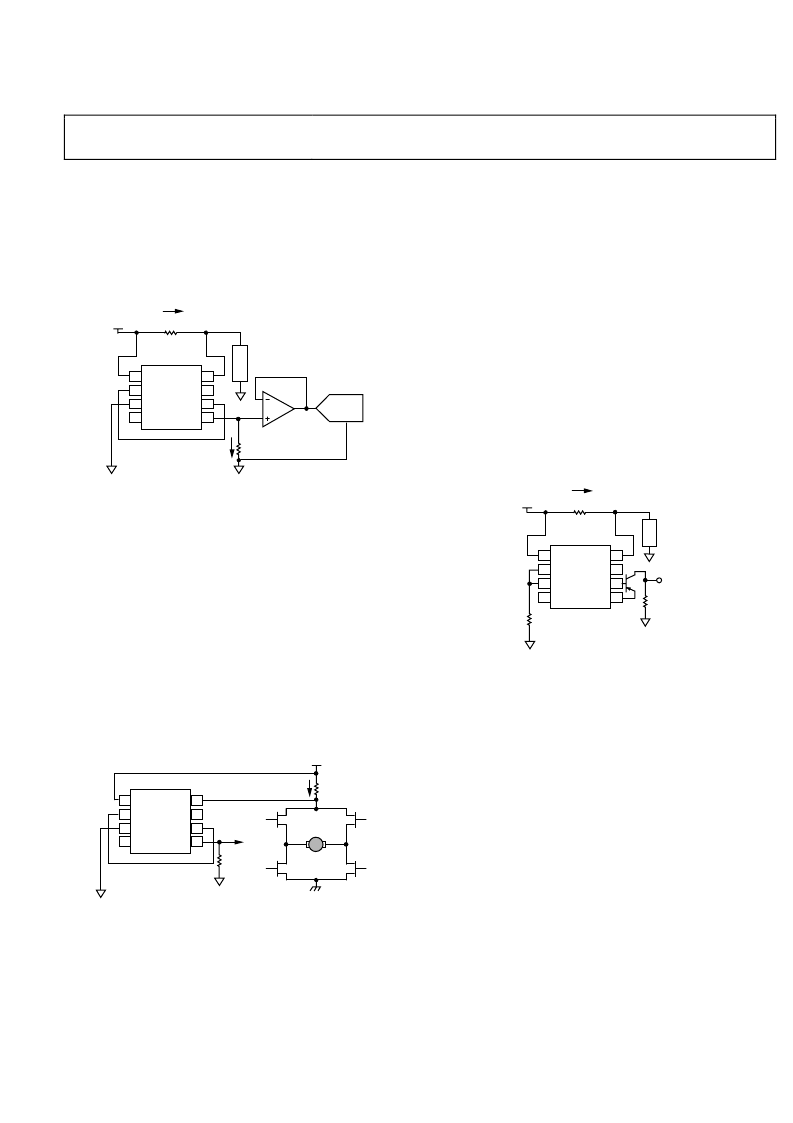
GENERAL HIGH-SIDE CURRENT SENSING
The AD8212 output is intended to drive high impedance nodes.
Therefore, if interfacing with a converter, it is recommended
that the output voltage across R
OUT
be buffered, so that the gain
of the AD8212 is not affected.
Rev. 0 | Page 11 of 16
AD8661
0
V+
1
COM
2
BIAS
3
NC
4
V
SENSE
8
NC
7
ALPHA
I
OUT
6
5
AD8212
I
LOAD
I
OUT
BATTERY
R
SHUNT
L
ADC
R
OUT
NOTES
1. NC = NO CONNECT.
Figure 24. Normal Voltage Range Operation
Careful calculations must be made when choosing a gain
resistor so as not to exceed the input voltage range of the
converter. The output of the AD8212 can be as high as
(V+) 5 V. However, the true output maximum voltage is
dependent upon the differential input voltage, and the resulting
output current across R
OUT
, which can be as high as 500 μA
(based on a 500 mV maximum input differential limit).
MOTOR CONTROL
The AD8212 is a practical solution for high-side current sensing
in motor control applications. In cases where the shunt resistor
is referenced to battery and the current flowing is unidirectional,
as shown in Figure 25, the AD8212 monitors the current with
no additional supply pin necessary.
0
R
OUT
MOTOR
V+
1
COM
2
BIAS
3
NC
4
V
SENSE
8
NC
7
ALPHA
I
OUT
6
5
AD8212
I
MOTOR
V
OUT
BATTERY
NOTES
1. NC = NO CONNECT.
Figure 25. High-Side Current Sensing for Motor Control
500 V CURRENT MONITOR
As noted in the High Voltage Operation Using an External PNP
Transistor section, the AD8212 common-mode voltage range is
extended by using an external PNP transistor. This mode of
operation is achievable with many amplifiers featuring a current
output. However, typically an external Zener regulator must be
added, along with a FET device, to withstand the common-mode
voltage and maintain output current accuracy.
The AD8212 features an integrated regulator (which acts as a
Zener regulator). It offers output current compensation that
allows the user to maintain excellent output current accuracy
by using any PNP transistor. Reliability is increased due to
lower component count. Most importantly, the output current
accuracy is high, allowing the user to choose an inexpensive
PNP transistor to withstand the increased common-mode
voltage.
0
V+
1
COM
2
BIAS
3
NC
4
V
SENSE
8
NC
7
ALPHA
I
OUT
6
5
AD8212
I
LOAD
500V
R
SHUNT
L
R
OUT
500k
VOUT
NOTES
1. TRANSISTOR V
BREAKDOWN
VOLTAGE MUST BE 500V.
2. NC = NO CONNECT.
Figure 26. High Voltage Operation Using External PNP
相關PDF資料 |
PDF描述 |
|---|---|
| AD8221AR-REEL | Single Supply, Rail-to-Rail, Low Cost Instrumentation Amplifier |
| AD8221AR-REEL7 | Single Supply, Rail-to-Rail, Low Cost Instrumentation Amplifier |
| AD8221ARM | Single Supply, Rail-to-Rail, Low Cost Instrumentation Amplifier |
| AD8221ARM-REEL | Single Supply, Rail-to-Rail, Low Cost Instrumentation Amplifier |
| AD8221ARM-REEL7 | Single Supply, Rail-to-Rail, Low Cost Instrumentation Amplifier |
相關代理商/技術參數 |
參數描述 |
|---|---|
| AD8212_07 | 制造商:AD 制造商全稱:Analog Devices 功能描述:High Voltage Current Shunt Monitor |
| AD8212AL/QMLR | 制造商:Analog Devices 功能描述: |
| AD8212AL-EMX | 制造商:Analog Devices 功能描述:ENGINEERING VERSION OF AD8212AL/QMLR - Rail/Tube |
| AD8212WYRMZ | 功能描述:IC CURRENT MONITOR 8MSOP RoHS:是 類別:集成電路 (IC) >> PMIC - 穩流/電流管理 系列:- 產品培訓模塊:Lead (SnPb) Finish for COTS Obsolescence Mitigation Program 標準包裝:50 系列:- 功能:電流開關 檢測方法:- 精確度:±10% 輸入電壓:1.7 V ~ 5.5 V 電流 - 輸出:600mA 工作溫度:-40°C ~ 125°C 安裝類型:表面貼裝 封裝/外殼:10-UFQFN 供應商設備封裝:10-UTQFN(1.4x1.8) 包裝:管件 |
| AD8212WYRMZ1 | 制造商:AD 制造商全稱:Analog Devices 功能描述:High Voltage Current Shunt Monitor |
發布緊急采購,3分鐘左右您將得到回復。