- 您現(xiàn)在的位置:買(mǎi)賣(mài)IC網(wǎng) > PDF目錄373941 > AD8212 (Analog Devices, Inc.) High Voltage Current Shunt Monitor PDF資料下載
參數(shù)資料
| 型號(hào): | AD8212 |
| 廠商: | Analog Devices, Inc. |
| 英文描述: | High Voltage Current Shunt Monitor |
| 中文描述: | 高壓電流分流監(jiān)控 |
| 文件頁(yè)數(shù): | 9/16頁(yè) |
| 文件大小: | 310K |
| 代理商: | AD8212 |
第1頁(yè)第2頁(yè)第3頁(yè)第4頁(yè)第5頁(yè)第6頁(yè)第7頁(yè)第8頁(yè)當(dāng)前第9頁(yè)第10頁(yè)第11頁(yè)第12頁(yè)第13頁(yè)第14頁(yè)第15頁(yè)第16頁(yè)
AD8212
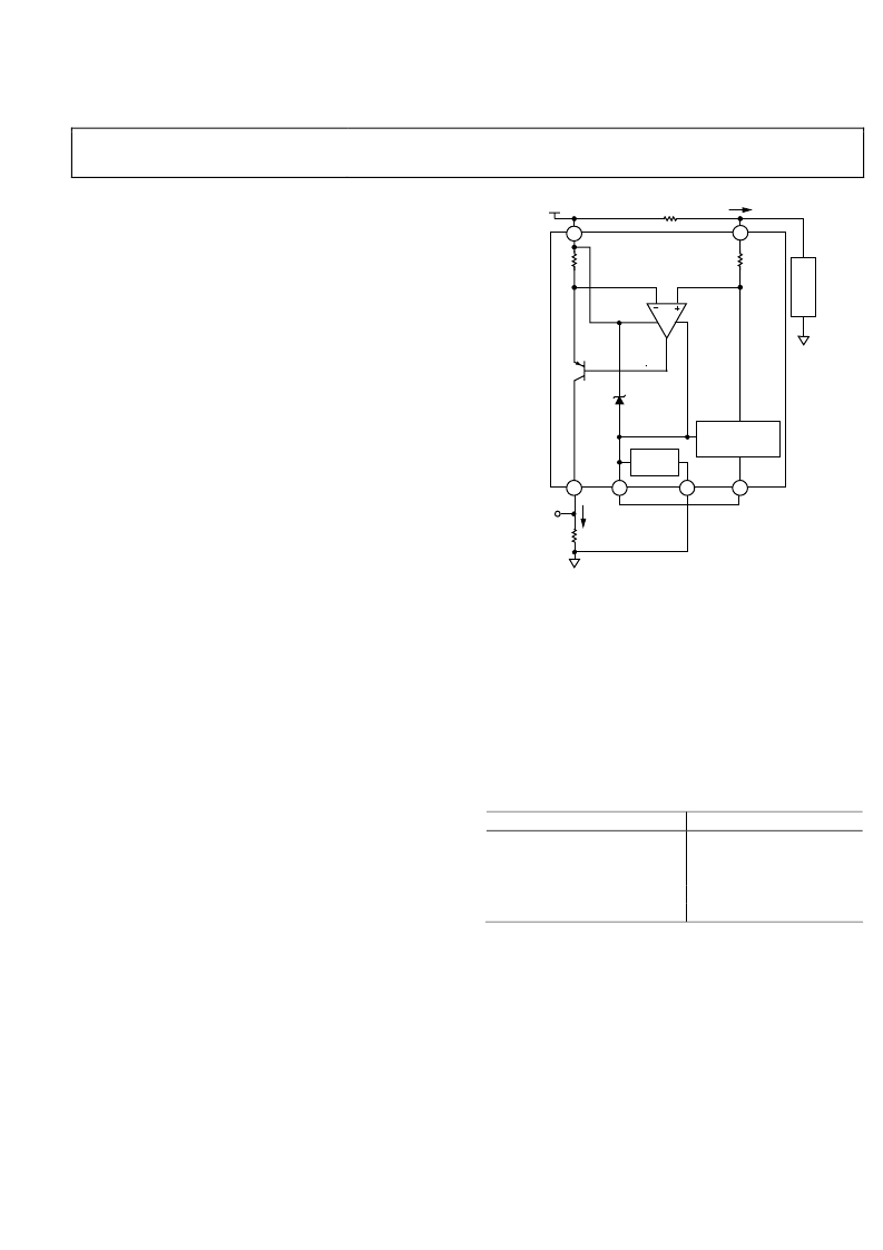
THEORY OF OPERATION
NORMAL OPERATION
(7 V TO 65 V SUPPLY (V+) RANGE)
In typical applications, the AD8212 measures a small
differential input voltage generated by a load current
flowing through a shunt resistor.
The operational amplifier (A1) is connected across the shunt
resistor (R
SHUNT
) with its inverting input connected to the
battery/supply side, and the noninverting input connected
to the load side of the system. Amplifier A1 is powered via
an internal series regulator (depicted as a Zener diode in
Figure 22). This regulator maintains a constant 5 V between
the battery/supply terminal of the AD8212 and COM (Pin 2),
which represents the lowest common point of the internal
circuitry.
A load current flowing through the external shunt resistor
produces a voltage at the input terminals of the AD8212.
Amplifier A1 responds by causing Transistor Q1 to conduct the
necessary current through Resistor R1 to equalize the potential
at both the inverting and noninverting inputs of Amplifier A1.
The current through the emitter of Transistor Q1 (I
OUT
) is
proportional to the input voltage (V
SENSE
), and, therefore, the
load current (I
LOAD
) through the shunt resistor (R
SHUNT
). The
output current (I
OUT
) is converted to a voltage by using an
external resistor, the value of which is dependent on the input
to output gain equation desired in the application.
The transfer function for the AD8212 is
I
OUT
= (
g
m
×
V
SENSE
)
V
SENSE
=
I
LOAD
×
R
SHUNT
V
OUT
=
I
OUT
×
R
OUT
V
OUT
= (V
SENSE
× R
OUT
)/
1000
where:
g
m
= 1000
μ
A/V.
In normal voltage operation mode, the bias circuit is connected
to GND, as shown in Figure 22. In this mode, I
BIAS
is typically
185 μA throughout the 7 V to 65 V (V+) range.
Rev. 0 | Page 9 of 16
I
OUT
I
LOAD
R
OUT
AD8212
BATTERY
R
SHUNT
0
1
8
5
2
3
6
OUTPUT
CURRENT
COMPENSATION
L
R1
R2
A1
Q1
VOUT
BIAS
CIRCUIT
Figure 22. Typical Connection (7 V to 65 V Supply (Pin V+) Range)
When using the AD8212 as described, the battery/supply
voltage in the system must be between 7 V to 65 V. The 7 V
minimum supply range is necessary to turn on the internal
regulator (shown as a Zener diode in Figure 22). This regulated
voltage then remains a constant 5 V, regardless of the supply
(V+) voltage. The 65 V maximum limit in this mode of
operation is due to the breakdown voltage limitation of the
AD8212 process.
Typically, a 1% resistor can be used to convert the output
current to a voltage. Table 4 provides suggested R
OUT
values.
Table 4. Suggested R
OUT
Values
Gain (V/V)
1
10
20
50
100
R
OUT
(kΩ)
1
10
20
49.9
100
相關(guān)PDF資料 |
PDF描述 |
|---|---|
| AD8221AR-REEL | Single Supply, Rail-to-Rail, Low Cost Instrumentation Amplifier |
| AD8221AR-REEL7 | Single Supply, Rail-to-Rail, Low Cost Instrumentation Amplifier |
| AD8221ARM | Single Supply, Rail-to-Rail, Low Cost Instrumentation Amplifier |
| AD8221ARM-REEL | Single Supply, Rail-to-Rail, Low Cost Instrumentation Amplifier |
| AD8221ARM-REEL7 | Single Supply, Rail-to-Rail, Low Cost Instrumentation Amplifier |
相關(guān)代理商/技術(shù)參數(shù) |
參數(shù)描述 |
|---|---|
| AD8212_07 | 制造商:AD 制造商全稱(chēng):Analog Devices 功能描述:High Voltage Current Shunt Monitor |
| AD8212AL/QMLR | 制造商:Analog Devices 功能描述: |
| AD8212AL-EMX | 制造商:Analog Devices 功能描述:ENGINEERING VERSION OF AD8212AL/QMLR - Rail/Tube |
| AD8212WYRMZ | 功能描述:IC CURRENT MONITOR 8MSOP RoHS:是 類(lèi)別:集成電路 (IC) >> PMIC - 穩(wěn)流/電流管理 系列:- 產(chǎn)品培訓(xùn)模塊:Lead (SnPb) Finish for COTS Obsolescence Mitigation Program 標(biāo)準(zhǔn)包裝:50 系列:- 功能:電流開(kāi)關(guān) 檢測(cè)方法:- 精確度:±10% 輸入電壓:1.7 V ~ 5.5 V 電流 - 輸出:600mA 工作溫度:-40°C ~ 125°C 安裝類(lèi)型:表面貼裝 封裝/外殼:10-UFQFN 供應(yīng)商設(shè)備封裝:10-UTQFN(1.4x1.8) 包裝:管件 |
| AD8212WYRMZ1 | 制造商:AD 制造商全稱(chēng):Analog Devices 功能描述:High Voltage Current Shunt Monitor |
發(fā)布緊急采購(gòu),3分鐘左右您將得到回復(fù)。