- 您現(xiàn)在的位置:買(mǎi)賣(mài)IC網(wǎng) > PDF目錄373942 > AD8302-EVAL (Analog Devices, Inc.) LF.2.7 GHz RF/IF Gain and Phase Detector PDF資料下載
參數(shù)資料
| 型號(hào): | AD8302-EVAL |
| 廠商: | Analog Devices, Inc. |
| 英文描述: | LF.2.7 GHz RF/IF Gain and Phase Detector |
| 中文描述: | LF.2.7 GHz射頻/中頻增益和相位檢波器 |
| 文件頁(yè)數(shù): | 18/24頁(yè) |
| 文件大小: | 533K |
| 代理商: | AD8302-EVAL |
第1頁(yè)第2頁(yè)第3頁(yè)第4頁(yè)第5頁(yè)第6頁(yè)第7頁(yè)第8頁(yè)第9頁(yè)第10頁(yè)第11頁(yè)第12頁(yè)第13頁(yè)第14頁(yè)第15頁(yè)第16頁(yè)第17頁(yè)當(dāng)前第18頁(yè)第19頁(yè)第20頁(yè)第21頁(yè)第22頁(yè)第23頁(yè)第24頁(yè)
REV. 0
AD8302
–18–
Cross-modulation of Magnitude and Phase
At high frequencies, unintentional cross coupling between signals
in channels A and B inevitably occurs due to on-chip and board-
level parasitics. When the two signals presented to the AD8302
inputs are at very different levels, the cross-coupling introduces
cross-modulation of the phase and magnitude responses. If the two
signals are held at the same relative levels and the phase between
them is modulated, then only the phase output should respond.
Due to phase-to-amplitude cross modulation, the magnitude out-
put shows a residual response. A similar effect occurs when the
relative phase is held constant while the magnitude difference is
modulated; i.e an expected magnitude response and a residual
phase response are observed due to amplitude-to-phase cross
modulation. The point where these effects are noticeable depends
on the signal frequency and the magnitude of the difference. Typi-
cally, for differences <20 dB, the effects of cross modulation are
negligible at 900 MHz.
Modifying the Slope and Center-Point
The default slope and center-point values can be modified with
the addition of external resistors. Since the output interface
blocks are generalized for both magnitude and phase functions,
the scaling modification techniques are equally valid for both
outputs. Figure 8 demonstrates how a simple voltage divider
from the VMAG and VPHS pins to the MSET and PSET pins
can be used to modify the slope. The increase in slope is given
by 1 + R1/(R2 20 k
). Note that it may be necessary to account
for the MSET and PSET input impedance of 20 k
which has a
±
20% manufacturing tolerance. As is generally true in such feed-
back systems, envelope bandwidth is decreased and the output
noise transferred from the input is increased by the same factor.
For example, by selecting R1 and R2 to be 10 k
and 20 k
,
respectively, gain slope increases from the nominal 30 mV/dB by
a factor of 2 to 60 mV/dB. The range is reduced by a factor of
two and the new center-point is at –15 dB; i.e. the range now
extends from –30 dB, corresponding to V
MAG
= 0 V, to 0 dB,
corresponding to V
MAG
= 1.8 V.
NEW SLOPE = 30mV/dB 1
R1
R2
||
R20k
VMAG
MSET
20k
R1
R2
Figure 8. Increasing the Slope Requires the Inclusion of a
Voltage Divider
Repositioning the center-point back to its original value of 0 dB
simply requires that an appropriate voltage be applied to the
grounded side of the lower resistor in the voltage divider. This
voltage may be provided externally or derived from the inter-
nal reference voltage on pin VREF. For the specific choice of
R2 = 20 k
, the center-point is easily readjusted to 0 dB by con-
necting the VREF pin directly to the lower pin of R2 as shown in
Figure 9. The increase in slope is now simplified to 1 + R1/10k
.
Since this 1.80 V reference voltage is derived from the same
bandgap reference that determines the nominal center-point,
their tracking with temperature, supply and part-to-part varia-
tions should be better in comparison to a fixed external voltage.
If the center-point is shifted to 0 dB in the previous example
where the slope was doubled, then the range spans from –15 dB
at V
MAG
= 0 V to 15 dB at V
MAG
= 1.8 V.
1
R1
10k
NEW SLOPE = 30mV/dB
VMAG
MSET
20k
R1
20k
VREF
Figure 9. The Center-Point is Repositioned with the Help
of the Internal Reference Voltage of 1.80 V
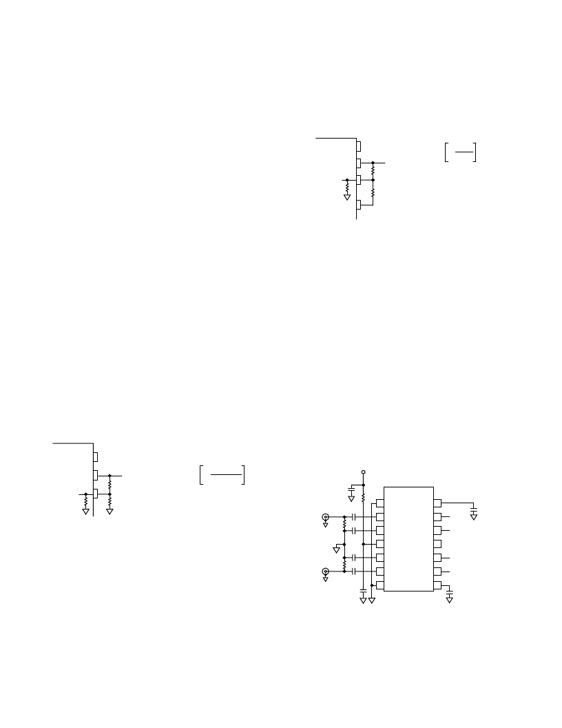
Comparator and Controller Modes
The AD8302 can also operate in a comparator mode if used in
the arrangement shown in Figure 10 where the DUT is the ele-
ment to be evaluated. The VMAG and VPHS pins are no longer
connected to MSET and PSET. The trip-point thresholds for
the gain and phase difference comparison are determined by the
voltages applied to pins MSET and PSET according to,
V
MSET
(
V
) = 30
mV
/
dB
×
Gain
SP
(
dB
) + 900
mV
V
PSET
(
V
)= –10
mV
/
°
×
(|
Phase
SP
(
°
)|–90
°
) + 900
mV
where
Gain
SP
(
dB
) and
Phase
SP
(
°
) are the desired gain and
phase thresholds. If the actual gain and phase between the two
input channels differ from these thresholds, the V
MAG
and V
PHS
outputs toggle like comparators; i.e.,
1.8
V
if Gain
>
Gain
SP
V
MAG
=
0
V
if
Gain
<
Gain
SP
(11)
(12)
(13)
1.8 V
if
Phase
>
Phase
SP
V
PHS
=
(14)
0 V
if
Phase
<
Phase
SP
V
MAG
V
MSET
V
PSET
V
PHS
1
COMM
MFLT
14
INPA
VMAG
2
13
OFSA
MSET
3
12
VPOS
VREF
4
11
OFSB
PSET
5
10
INPB
VPHS
6
9
COMM
PFLT
7
8
AD8302
C2
C8
C1
C4
C6
C5
R1
R2
V
INA
V
INB
VP
C7
R4
C3
Figure 10. Disconnecting the Feedback to the Setpoint
Controls, the AD8302 Operates in Comparator Mode
相關(guān)PDF資料 |
PDF描述 |
|---|---|
| AD8302ARU | LF.2.7 GHz RF/IF Gain and Phase Detector |
| AD8302ARU-REEL7 | LF.2.7 GHz RF/IF Gain and Phase Detector |
| AD8303 | Dual, Serial Input Complete 12-Bit DAC(串行輸入雙12位D/A轉(zhuǎn)換器) |
| AD8304ARU-REEL | 160 dB Range (100 pA -10 mA) Logarithmic Converter |
| AD8304 | 160 dB Range (100 pA -10 mA) Logarithmic Converter |
相關(guān)代理商/技術(shù)參數(shù) |
參數(shù)描述 |
|---|---|
| AD8302-EVALZ | 功能描述:EVALUATION BOARD FOR AD8302 RoHS:是 類(lèi)別:RF/IF 和 RFID >> RF 評(píng)估和開(kāi)發(fā)套件,板 系列:- 標(biāo)準(zhǔn)包裝:1 系列:- 類(lèi)型:GPS 接收器 頻率:1575MHz 適用于相關(guān)產(chǎn)品:- 已供物品:模塊 其它名稱:SER3796 |
| AD8303 | 制造商:Analog Devices 功能描述: |
| AD8303AN | 制造商:AD 制造商全稱:Analog Devices 功能描述:+3 V, Dual, Serial Input Complete 12-Bit DAC |
| AD8303AR | 制造商:Analog Devices 功能描述:IC 12-BIT DAC |
| AD8303AR-REEL | 制造商:Analog Devices 功能描述:DAC 2-CH R-2R 12-bit 14-Pin SOIC N T/R 制造商:Rochester Electronics LLC 功能描述:IC,DUAL 12BIT,+3V,COMPLETE DAC,TAPE&REEL - Tape and Reel |
發(fā)布緊急采購(gòu),3分鐘左右您將得到回復(fù)。