- 您現在的位置:買賣IC網 > PDF目錄373942 > AD8303 (Analog Devices, Inc.) Dual, Serial Input Complete 12-Bit DAC(串行輸入雙12位D/A轉換器) PDF資料下載
參數資料
| 型號: | AD8303 |
| 廠商: | Analog Devices, Inc. |
| 英文描述: | Dual, Serial Input Complete 12-Bit DAC(串行輸入雙12位D/A轉換器) |
| 中文描述: | 雙通道,串行輸入完整的12位DAC(串行輸入雙12位的D / A轉換器) |
| 文件頁數: | 1/16頁 |
| 文件大小: | 378K |
| 代理商: | AD8303 |
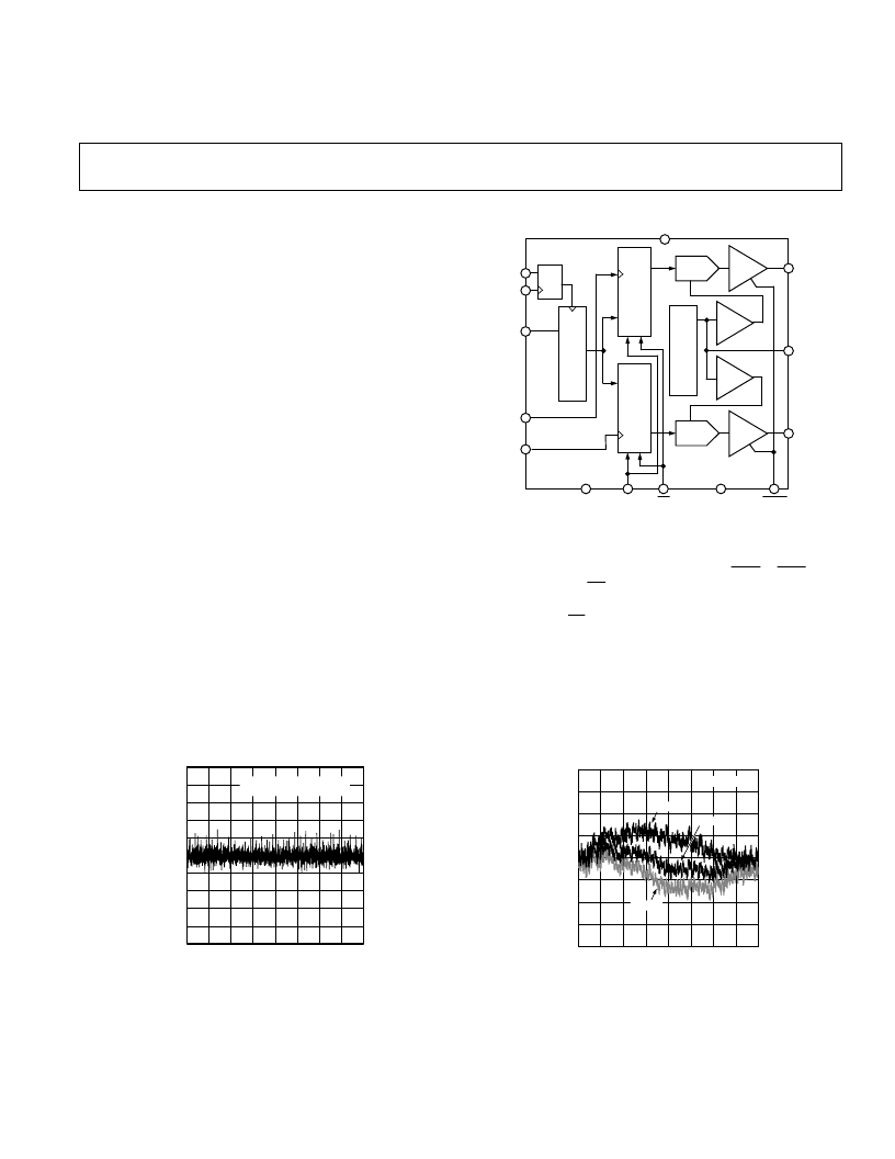
FUNCTIONAL BLOCK DIAGRAM
D
A
C
A
R
E
G
I
S
T
E
R
R
D
P
En
S
H
I
F
T
R
E
G
I
S
T
E
R
D
A
C
B
R
E
G
I
S
T
E
R
R
D
P
R
E
F
E
R
E
N
C
E
B
A
N
D
G
A
P
DAC A
DAC B
V
DD
REF
REF
AD8303
V
OUTA
V
REF
V
OUTB
CS
CLK
SDI
(DATA)
LDA
LDB
DGND
MSB
RS
AGND
SHDN
OP
A
OP
B
REV. 0
Information furnished by Analog Devices is believed to be accurate and
reliable. However, no responsibility is assumed by Analog Devices for its
use, nor for any infringements of patents or other rights of third parties
which may result from its use. No license is granted by implication or
otherwise under any patent or patent rights of Analog Devices.
a
+3 V, Dual, Serial Input
Complete 12-Bit DAC
AD8303
Analog Devices, Inc., 1996
One Technology Way, P.O. Box 9106, Norwood, MA 02062-9106, U.S.A.
Tel: 617/329-4700
Fax: 617/326-8703
FEATURES
Complete Dual 12-Bit DAC
Pretrimmed Internal Voltage Reference
Single +3 V Operation
0.5 mV/Bit with 2.0475 V Full Scale
Low Power: 9.6 mW
3-Wire Serial SPI Compatible Interface
Power Shutdown I
DD
< 1
m
A
Compact SO-14, 1.75 mm Height Package
APPLICATIONS
Portable Communications
Digitally Controlled Calibration
Servo Controls
PC Peripherals
GENERAL DESCRIPTION
The AD8303 is a complete (includes internal reference) dual,
12-bit, voltage output digital-to-analog converter designed to
operate from a single +3 volt supply. Built using a CBCMOS
process, this monolithic DAC offers the user low cost and ease-
of-use in single-supply +3 volt systems. Operation is guaranteed
over the supply voltage range of +2.7 V to +5.5 V making this
device ideal for battery operated applications.
The 2.0475 V full-scale voltage output is laser-trimmed to
maintain accuracy over the operating temperature range of the
device. The binary input data format provides an easy-to-use
one-half millivolt-per-bit software programmability. The voltage
outputs are capable of sourcing 3 mA.
DIGITAL INPUT CODE – Decimal
D
1.0
–1.0
0
4096
1024
2048
3072
0.8
0.2
0
–0.4
–0.8
0.6
0.4
–0.2
–0.6
V
DD
= +5V
T
A
= –40
°
C, +25
°
C, +85
°
C
Figure 1. Differential Nonlinearity Error vs. Code
A double buffered serial data interface offers high speed, three-
wire, DSP and SPI microcontroller compatible inputs using
data in (SDI), clock (CLK) and load strobe (
LDA
+
LDB
)
pins. A chip-select (
CS
) pin simplifies connection of multiple
DAC packages by enabling the clock input when active low.
Additionally, an
RS
input sets the output to zero scale or to 1/2
scale based on the level applied to the MSB pin. A power
shutdown feature reduces power dissipation to less than 3
μ
W.
The AD8303 is specified over the extended industrial (–40
°
C to
+85
°
C) temperature range. AD8303s are available in plastic
DIP and low profile 1.75 mm height SO-14 surface mount
packages. For single-channel DAC applications, see the
AD8300 which is offered in the 8-lead DIP and SO-8 packages.
DIGITAL INPUT CODE – Decimal
I
2
–2
1.5
0
–0.5
–1
–1.5
1
0.5
V
DD
= +5V
0
1024
2048
3072
4096
+25
°
C
+85
°
C
–40
°
C
Figure 2. Linearity Error vs. Digital Code and Temperature
相關PDF資料 |
PDF描述 |
|---|---|
| AD8304ARU-REEL | 160 dB Range (100 pA -10 mA) Logarithmic Converter |
| AD8304 | 160 dB Range (100 pA -10 mA) Logarithmic Converter |
| AD8304-EVAL | 160 dB Range (100 pA -10 mA) Logarithmic Converter |
| AD8304ARU | 160 dB Range (100 pA -10 mA) Logarithmic Converter |
| AD8304ARU-REEL7 | 160 dB Range (100 pA -10 mA) Logarithmic Converter |
相關代理商/技術參數 |
參數描述 |
|---|---|
| AD8303AN | 制造商:AD 制造商全稱:Analog Devices 功能描述:+3 V, Dual, Serial Input Complete 12-Bit DAC |
| AD8303AR | 制造商:Analog Devices 功能描述:IC 12-BIT DAC |
| AD8303AR-REEL | 制造商:Analog Devices 功能描述:DAC 2-CH R-2R 12-bit 14-Pin SOIC N T/R 制造商:Rochester Electronics LLC 功能描述:IC,DUAL 12BIT,+3V,COMPLETE DAC,TAPE&REEL - Tape and Reel |
| AD8303ARZ-REEL | 功能描述:IC DAC 12BIT SERIAL 14SOIC RoHS:是 類別:集成電路 (IC) >> 數據采集 - 數模轉換器 系列:- 標準包裝:2,400 系列:- 設置時間:- 位數:18 數據接口:串行 轉換器數目:3 電壓電源:模擬和數字 功率耗散(最大):- 工作溫度:-40°C ~ 85°C 安裝類型:表面貼裝 封裝/外殼:36-TFBGA 供應商設備封裝:36-TFBGA 包裝:帶卷 (TR) 輸出數目和類型:* 采樣率(每秒):* |
| AD8303JRU | 制造商:Analog Devices 功能描述:DAC 2-CH R-2R 12-bit 14-Pin TSSOP 制造商:Rochester Electronics LLC 功能描述:IC,DUAL 12BIT,+3V,COMPLETE DAC - Bulk |
發布緊急采購,3分鐘左右您將得到回復。