- 您現(xiàn)在的位置:買賣IC網(wǎng) > PDF目錄373942 > AD8303 (Analog Devices, Inc.) Dual, Serial Input Complete 12-Bit DAC(串行輸入雙12位D/A轉換器) PDF資料下載
參數(shù)資料
| 型號: | AD8303 |
| 廠商: | Analog Devices, Inc. |
| 英文描述: | Dual, Serial Input Complete 12-Bit DAC(串行輸入雙12位D/A轉換器) |
| 中文描述: | 雙通道,串行輸入完整的12位DAC(串行輸入雙12位的D / A轉換器) |
| 文件頁數(shù): | 8/16頁 |
| 文件大小: | 378K |
| 代理商: | AD8303 |
AD8303
REV. 0
–8–
THEORY OF OPERATION
The AD8303 is a complete, ready-to-use, dual, 12-bit digital-to-
analog converter. Only one +2.7 V to +5.5 V power supply is
necessary for operation. It contains two voltage-switched, 12-bit,
laser-trimmed digital-to-analog converters, a curvature-
corrected bandgap reference, rail-to-rail output op amps, input
shift register, and two DAC registers. The serial data interface
consists of a serial data input (SDI), clock (CLK), chip select
(
CS
) and two DAC load strobe pins (
LDA
and
LDB
).
For battery operation and similar low power applications, a
shutdown feature (
SHDN
) is available to reduce power supply
current to less than 1
μ
A. In addition an asynchronous reset pin
(
RS
) will set both DAC outputs to either zero volts or to
midscale, depending on the logic value applied to the MSB pin.
This function is useful for power-on reset or system failure
recovery to a known state.
D/A CONVERTER SECTION
Each of the two DACs is a 12-bit device with an output that
swings from GND potential to 0.4 V generated from the internal
bandgap voltage (Figure 22). Each DAC uses a laser-trimmed
segmented R-2R ladder that is switched by n-channel
MOSFETs. The output voltage of the DAC has a constant
resistance independent of digital input code. The DAC output is
internally connected to the rail-to-rail output op amp.
12-BIT DAC
2.5k
10k
V
2.047V
FS
BANDGAP
REF
1.0V
0.4V
0.4V
FS
V
1.0V
2k
10k
Figure 22. AD8303 Equivalent Schematic of Analog Section
AMPLIFIER SECTION
The internal DAC’s output is buffered by a low power
consumption, precision amplifier. This low power amplifier
contains a differential PNP pair input stage that provides low
offset voltage and low noise, as well as the ability to amplify the
zero-scale DAC output voltages, The rail-to-rail amplifier is
configured with a gain of approximately five in order to set the
2.0475 volt full-scale output (0.5 mV/LSB). An equivalent
circuit schematic for the amplifier section is shown in Figure 22.
The op amp has a 4
μ
s typical settling time to 0.1% of full scale.
There are slight differences in settling time for negative slewing
signals versus positive. Also, negative transition settling time to
within the last 6 LSBs of zero volts has an extended settling
time. See the oscilloscope photos in the typical performances
section of this data sheet.
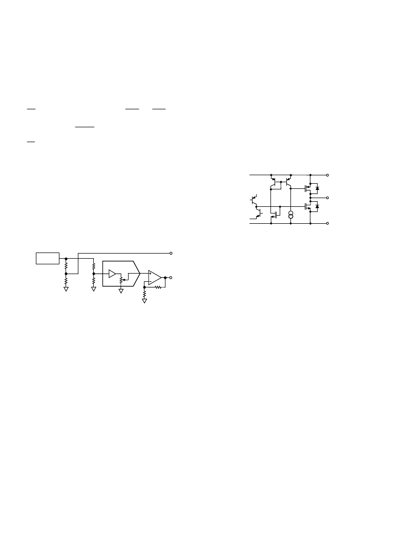
OUTPUT SECTION
The rail-to-rail output stage of this amplifier has been designed
to provide precision performance while operating near either
power supply. Figure 23 shows an equivalent output schematic
of the rail-to-rail amplifier with its N-channel pull-down FETs
that will pull an output load directly to GND. The output
sourcing current is provided by a P-channel pull-up device that
can source current to GND terminated loads.
The rail-to-rail output stage permits operation at supply
voltages down to +2.7 V. The N-channel output pull-down
MOSFET shown in Figure 23 has a 35
ON resistance which
sets the sink current capability near ground. In addition to
resistive load driving capability, the amplifier has also been
carefully designed and characterized for up to 500 pF capacitive
load driving capability.
P-CH
N-CH
V
DD
V
OUT
AGND
Figure 23. Equivalent Analog Output Circuit
REFERENCE SECTION
The internal curvature-corrected bandgap voltage reference is
laser trimmed for both initial accuracy and low temperature
coefficient. Figure 18 provides a histogram of total output
performance of full-scale versus temperature, which is dominated
by the reference performance.
V
REF
Output
The internal reference drives two resistor-divider networks. One
divider provides a 0.4 V reference for the DAC. The second
divider is trimmed to 1.0 V and is available at the V
REF
pin. The
V
REF
output is useful for ratiometric applications, and also for
generating a “false ground” or bipolar offset. See Figures 30
and Figure 31 for typical applications. Since V
REF
has a high
output impedance, it must be buffered if it is required to deliver
current to an external load.
相關PDF資料 |
PDF描述 |
|---|---|
| AD8304ARU-REEL | 160 dB Range (100 pA -10 mA) Logarithmic Converter |
| AD8304 | 160 dB Range (100 pA -10 mA) Logarithmic Converter |
| AD8304-EVAL | 160 dB Range (100 pA -10 mA) Logarithmic Converter |
| AD8304ARU | 160 dB Range (100 pA -10 mA) Logarithmic Converter |
| AD8304ARU-REEL7 | 160 dB Range (100 pA -10 mA) Logarithmic Converter |
相關代理商/技術參數(shù) |
參數(shù)描述 |
|---|---|
| AD8303AN | 制造商:AD 制造商全稱:Analog Devices 功能描述:+3 V, Dual, Serial Input Complete 12-Bit DAC |
| AD8303AR | 制造商:Analog Devices 功能描述:IC 12-BIT DAC |
| AD8303AR-REEL | 制造商:Analog Devices 功能描述:DAC 2-CH R-2R 12-bit 14-Pin SOIC N T/R 制造商:Rochester Electronics LLC 功能描述:IC,DUAL 12BIT,+3V,COMPLETE DAC,TAPE&REEL - Tape and Reel |
| AD8303ARZ-REEL | 功能描述:IC DAC 12BIT SERIAL 14SOIC RoHS:是 類別:集成電路 (IC) >> 數(shù)據(jù)采集 - 數(shù)模轉換器 系列:- 標準包裝:2,400 系列:- 設置時間:- 位數(shù):18 數(shù)據(jù)接口:串行 轉換器數(shù)目:3 電壓電源:模擬和數(shù)字 功率耗散(最大):- 工作溫度:-40°C ~ 85°C 安裝類型:表面貼裝 封裝/外殼:36-TFBGA 供應商設備封裝:36-TFBGA 包裝:帶卷 (TR) 輸出數(shù)目和類型:* 采樣率(每秒):* |
| AD8303JRU | 制造商:Analog Devices 功能描述:DAC 2-CH R-2R 12-bit 14-Pin TSSOP 制造商:Rochester Electronics LLC 功能描述:IC,DUAL 12BIT,+3V,COMPLETE DAC - Bulk |
發(fā)布緊急采購,3分鐘左右您將得到回復。