- 您現在的位置:買賣IC網 > PDF目錄373942 > AD8304-EVAL (Analog Devices, Inc.) 160 dB Range (100 pA -10 mA) Logarithmic Converter PDF資料下載
參數資料
| 型號: | AD8304-EVAL |
| 廠商: | Analog Devices, Inc. |
| 英文描述: | 160 dB Range (100 pA -10 mA) Logarithmic Converter |
| 中文描述: | 160分貝范圍(100功率放大器-10毫安)對數轉換器 |
| 文件頁數: | 13/20頁 |
| 文件大小: | 4286K |
| 代理商: | AD8304-EVAL |
REV. A
AD8304
–13–
The use of a capacitor at the VLOG Pin to create a single-pole
filter has already been mentioned. The small added cost of the few
external components needed to realize a multipole filter is often
justified in a high performance measurement system. Figure 8
shows a Sallen-Key filter structure. Here, the resistor needed at
the front of the network is provided entirely by the accurate 5 k
present at the VLOG output; R
B
will have a similar value. The corner
frequency and Q (damping factor) are determined by the capacitors
C
A
and C
B
and the gain G = (R
A
+ R
B
)/R
B
. A suggested starting
point for choosing these components using various gains is pro-
vided in Table IV; the values shown are for a 1 kHz corner (also
see TPC 12). This frequency can be increased or decreased by
scaling the capacitor values. Note that R
D
, G, and the capacitor ratio
C
A
/C
B
should not deviate from the suggested values to maintain the
shape of the ac amplitude response and pulse overshoot provided
by the values shown in this table. In all cases, the roll-off rate above
the corner is 40 dB/dec.
6
3
4
PDB
BIAS
VREF
10
2
12
VPDB
VSUM
INPT
VSUM
5
1
VNEG
~10k
ACOM
14
VPS2
PWDN
VPS1
VREF
7
VLOG
8
BFIN
9
BFNG
TEMPERATURE
COMPENSATION
5k
11
VOUT
0.5V
I
PD
NC
R1
750k
10nF
C1
1nF
13
RA
V
P
V
OUT
NC = NO CONNECT
CA
RD
RB
CB
Figure 8. Two-Pole Low-Pass Filter
Table IV. Two-Pole Filter Parameters for 1 kHz Cutoff
Frequency
*
R
A
(k )
R
B
(k )
V
Y
(V/decade)
R
D
(k )
C
A
(nF)
C
B
(nF)
G
0
10
12
24
open
10
8
6
1
2
2.5
5
0.2
0.4
0.5
1.0
11.3
6.02
12.1
10.0
12
33
33
33
12
22
18
18
The corner frequency can be adjusted by scaling capacitors C
and C
. For
example, to reduce the corner frequency to 100 Hz, raise the values of C
A
and
C
by 10
.
*See TPC 12.
Operation in Comparator Modes
In certain applications, the need may arise to generate a logical
output when the input current has reached a certain value. This
can be easily addressed by using a fraction of the voltage refer-
ence to provide the setpoint (threshold) and using the buffer
without feedback in a comparator mode, as illustrated in Figure 9.
Since V
LOG
runs from ground up to 1.6 V maximum, the 2 V
reference is more than adequate to cover the full dynamic range
of I
PD
. Note that the threshold for an increasing I
PD
is unchanged,
while the release point for decreasing currents is 5 dB below
this. Raising R
H
to 5 M
reduces the hysteresis to 0.5 dB, or it
may be increased using a lower value for R
H
.
6
3
4
PDB
BIAS
VREF
10
2
12
VPDB
VSUM
INPT
VSUM
5
1
~10k
ACOM
14
VPS2
PWDN
VPS1
VREF
7
VLOG
8
BFIN
9
BFNG
TEMPERATURE
COMPENSATION
5k
11
VOUT
0.5V
I
PD
NC
R1
750
10nF
C1
13
V
P
NC = NO CONNEVNEG
RH
RG
RA
V
OUT
Figure 9. Using the Buffer as a Comparator
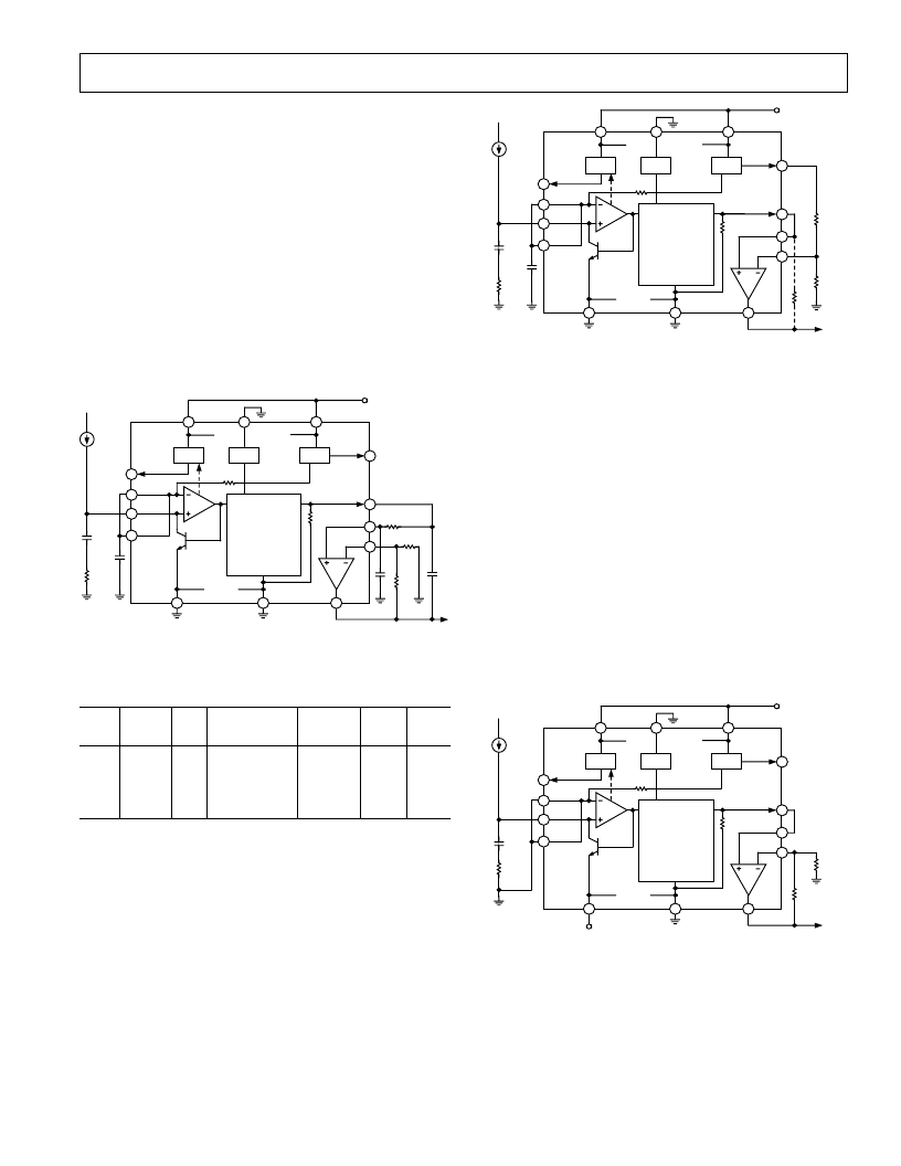
Using a Negative Supply
Most applications of the AD8304 will require only a single supply
of 3.0 V to 5.5 V. However, to provide further versatility, dual
supplies may be employed, as illustrated in Figure 10.
The use of a negative supply, V
N
, allows the summing node to
be placed exactly at ground level, because the input transistor
(Q1 in Figure 1) will have a negative bias on its emitter. V
N
may
be as small as
–
0.5 V, making the V
CE
the same as for the default
case. This bias need not be accurate, and a poorly defined source
can be used.
A larger supply of up to
–
5 V may be used. The effect on scaling
is minor. It merely moves the intercept by ~0.01 dB/V. Accord-
ingly, an uncertainty of 0.2 V in V
N
would result in a negligible
error of 0.002 dB. The slope is unaffected by V
N
. The log lin-
earity will be degraded at the extremes of the dynamic range as
indicated in Figure 11. The bias current, buffer output (and its
load) current, and the full I
PD
all have to be absorbed by this
negative supply, and its supply capacity must be ensured for the
maximum current condition.
6
3
4
PDB
BIAS
VREF
10
2
12
VPDB
VSUM
INPT
VSUM
5
1
VNEG
~10k
ACOM
14
VPS2
PWDN
VPS1
VREF
7
VLOG
8
BFIN
9
BFNG
TEMPERATURE
COMPENSATION
5k
11
VOUT
0.5V
I
PD
NC
R1
750
C1
13
V
P
NC = NO CONNECT
RB
RA
V
OUT
V
N
(–0.5V TO –3V)
Figure 10. Using a Negative Supply
With the summing node at ground, the AD8304 may now be used
as a voltage-input log amp, simply by inserting a suitably scaled
resistor from the voltage source to the
INPT Pin. The logarith-
mic accuracy for small voltages is limited by the offset of the JFET
op amp, appearing between this pin and VSUM.
The use of a negative supply also allows the output to swing below
ground, thereby allowing the intercept to correspond to a midrange
value of I
PD
. However, the voltage V
LOG
remains referenced to the
相關PDF資料 |
PDF描述 |
|---|---|
| AD8304ARU | 160 dB Range (100 pA -10 mA) Logarithmic Converter |
| AD8304ARU-REEL7 | 160 dB Range (100 pA -10 mA) Logarithmic Converter |
| AD8305 | 100 dB Range (10 nA to 1 mA) Logarithmic Converter |
| AD8305ACP | 100 dB Range (10 nA to 1 mA) Logarithmic Converter |
| AD8305ACP-REEL7 | 100 dB Range (10 nA to 1 mA) Logarithmic Converter |
相關代理商/技術參數 |
參數描述 |
|---|---|
| AD8304-EVALZ | 制造商:Analog Devices 功能描述:Evaluation Kit For 160 DB Range Logarithmic Converter 制造商:Analog Devices 功能描述:EVAL KIT FOR 160 DB RANGE (100 PA -10 MA) LOGARITHMIC CNVRTR - Bulk 制造商:Analog Devices 功能描述:EVAL LOGARITHMIC DECTECTOR AD8304 |
| AD8304XRU | 制造商:Analog Devices 功能描述: |
| AD8305 | 制造商:Analog Devices 功能描述:SP AMP LOG AMP SGL R-R O/P 6V/12V 16LFCSP EP - Bulk |
| AD8305_CSURF | 制造商:Analog Devices 功能描述: |
| AD8305ACP | 制造商:AD 制造商全稱:Analog Devices 功能描述:100 dB Range (10 nA to 1 mA) Logarithmic Converter |
發布緊急采購,3分鐘左右您將得到回復。