- 您現在的位置:買賣IC網 > PDF目錄373942 > AD8304-EVAL (Analog Devices, Inc.) 160 dB Range (100 pA -10 mA) Logarithmic Converter PDF資料下載
參數資料
| 型號: | AD8304-EVAL |
| 廠商: | Analog Devices, Inc. |
| 英文描述: | 160 dB Range (100 pA -10 mA) Logarithmic Converter |
| 中文描述: | 160分貝范圍(100功率放大器-10毫安)對數轉換器 |
| 文件頁數: | 3/20頁 |
| 文件大小: | 4286K |
| 代理商: | AD8304-EVAL |
REV. A
AD8304
–3–
CAUTION
ESD (electrostatic discharge) sensitive device. Electrostatic charges as high as 4000 V readily
accumulate on the human body and test equipment and can discharge without detection. Although the
AD8304 features proprietary ESD protection circuitry, permanent damage may occur on devices
subjected to high energy electrostatic discharges. Therefore, proper ESD precautions are recommended
to avoid performance degradation or loss of functionality.
WARNING!
ESD SENSITIVE DEVICE
ABSOLUTE MAXIMUM RATINGS
*
Supply Voltage V
P
–
V
N
. . . . . . . . . . . . . . . . . . . . . . . . . . . 8 V
Input Current . . . . . . . . . . . . . . . . . . . . . . . . . . . . . . . 20 mA
Internal Power Dissipation . . . . . . . . . . . . . . . . . . . . 270 mW
JA
. . . . . . . . . . . . . . . . . . . . . . . . . . . . . . . . . . . . . . 150
°
C/W
Maximum Junction Temperature . . . . . . . . . . . . . . . . 125
°
C
Operating Temperature Range . . . . . . . . . . .
–
40
°
C to +85
°
C
Storage Temperature Range . . . . . . . . . . . .
–
65
°
C to +150
°
C
Lead Temperature Range (Soldering 60 sec) . . . . . . . . 300
°
C
*
Stresses above those listed under Absolute Maximum Ratings may cause perma-
nent damage to the device. This is a stress rating only; functional operation of the
device at these or any other conditions above those indicated in the operational
section of this specification is not implied. Exposure to absolute maximum rating
conditions for extended periods may affect device reliability.
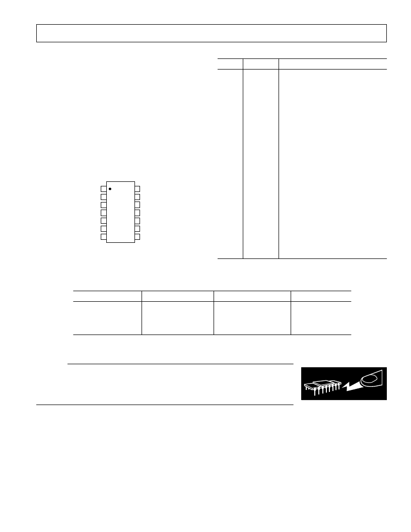
PIN FUNCTION DESCRIPTIONS
Pin No.
Mnemonic Function
1
VNEG
Optional Negative Supply, V
N
. This
pin is usually grounded; for details of
usage, see Applications section.
Power-Down Control Input. Device is
active when PWDN is taken LOW.
Guard Pins. Used to shield the INPT
current line.
Photodiode Current Input. Usually
connected to photodiode anode (the
photo current flows toward INPT).
Photodiode Biaser Output. May be
connected to photodiode cathode to
provide adaptive bias control.
Voltage Reference Output of 2 V
Output of the Logarithmic Front-End
Processor; R
OUT
= 5 k
to ground.
Buffer Amplifier Noninverting Input
(High Impedance)
Positive Supply, V
P
(3.0 V to 5.5 V)
Buffer Output; Low Impedance
Positive Supply, V
P
(3.0 V to 5.5 V)
Buffer Amplifier Inverting Input
Analog Ground
2
PWDN
3, 5
VSUM
4
INPT
6
VPDB
7
8
VREF
VLOG
9
BFIN
10
11
12
13
14
VPS2
VOUT
VPS1
BFNG
ACOM
PIN CONFIGURATION
(Not to Scale)
AD8304
VNEG
PWDN
VSUM
INPT
VSUM
VPDB
VREF
ACOM
BFNG
VPS1
VOUT
VPS2
BFIN
VLOG
1
2
3
4
5
6
7
14
13
12
11
10
9
8
ORDERING GUIDE
Model
Temperature Range
–
40
°
C to +85
°
C
Package Description
Package Option
AD8304ARU
AD8304ARU-REEL
AD8304ARU-REEL7
AD8304-EVAL
Tube, 14-Lead TSSOP
13" Tape and Reel
7" Tape and Reel
Evaluation Board
RU-14
相關PDF資料 |
PDF描述 |
|---|---|
| AD8304ARU | 160 dB Range (100 pA -10 mA) Logarithmic Converter |
| AD8304ARU-REEL7 | 160 dB Range (100 pA -10 mA) Logarithmic Converter |
| AD8305 | 100 dB Range (10 nA to 1 mA) Logarithmic Converter |
| AD8305ACP | 100 dB Range (10 nA to 1 mA) Logarithmic Converter |
| AD8305ACP-REEL7 | 100 dB Range (10 nA to 1 mA) Logarithmic Converter |
相關代理商/技術參數 |
參數描述 |
|---|---|
| AD8304-EVALZ | 制造商:Analog Devices 功能描述:Evaluation Kit For 160 DB Range Logarithmic Converter 制造商:Analog Devices 功能描述:EVAL KIT FOR 160 DB RANGE (100 PA -10 MA) LOGARITHMIC CNVRTR - Bulk 制造商:Analog Devices 功能描述:EVAL LOGARITHMIC DECTECTOR AD8304 |
| AD8304XRU | 制造商:Analog Devices 功能描述: |
| AD8305 | 制造商:Analog Devices 功能描述:SP AMP LOG AMP SGL R-R O/P 6V/12V 16LFCSP EP - Bulk |
| AD8305_CSURF | 制造商:Analog Devices 功能描述: |
| AD8305ACP | 制造商:AD 制造商全稱:Analog Devices 功能描述:100 dB Range (10 nA to 1 mA) Logarithmic Converter |
發布緊急采購,3分鐘左右您將得到回復。