- 您現在的位置:買賣IC網 > PDF目錄373942 > AD8304-EVAL (Analog Devices, Inc.) 160 dB Range (100 pA -10 mA) Logarithmic Converter PDF資料下載
參數資料
| 型號: | AD8304-EVAL |
| 廠商: | Analog Devices, Inc. |
| 英文描述: | 160 dB Range (100 pA -10 mA) Logarithmic Converter |
| 中文描述: | 160分貝范圍(100功率放大器-10毫安)對數轉換器 |
| 文件頁數: | 16/20頁 |
| 文件大小: | 4286K |
| 代理商: | AD8304-EVAL |
REV. A
–16–
AD8304
6
3
4
PDB
BIAS
VREF
10
2
12
VPDB
VSUM
INPT
VSUM
5
1
VNEG
~10k
ACOM
14
VPS2
PWDN
VPS1
VREF
7
VLOG
8
BFIN
9
BFNG
TEMPERATURE
COMPENSATION
5k
11
VOUT
0.5V
I
PD
NC
R1
750
C1
1nF
13
V
P
NC = NO CONNECT
RB
V
OUT
V
N
(–0.5V TO –3V)
10nF
V
OFS
AD8304
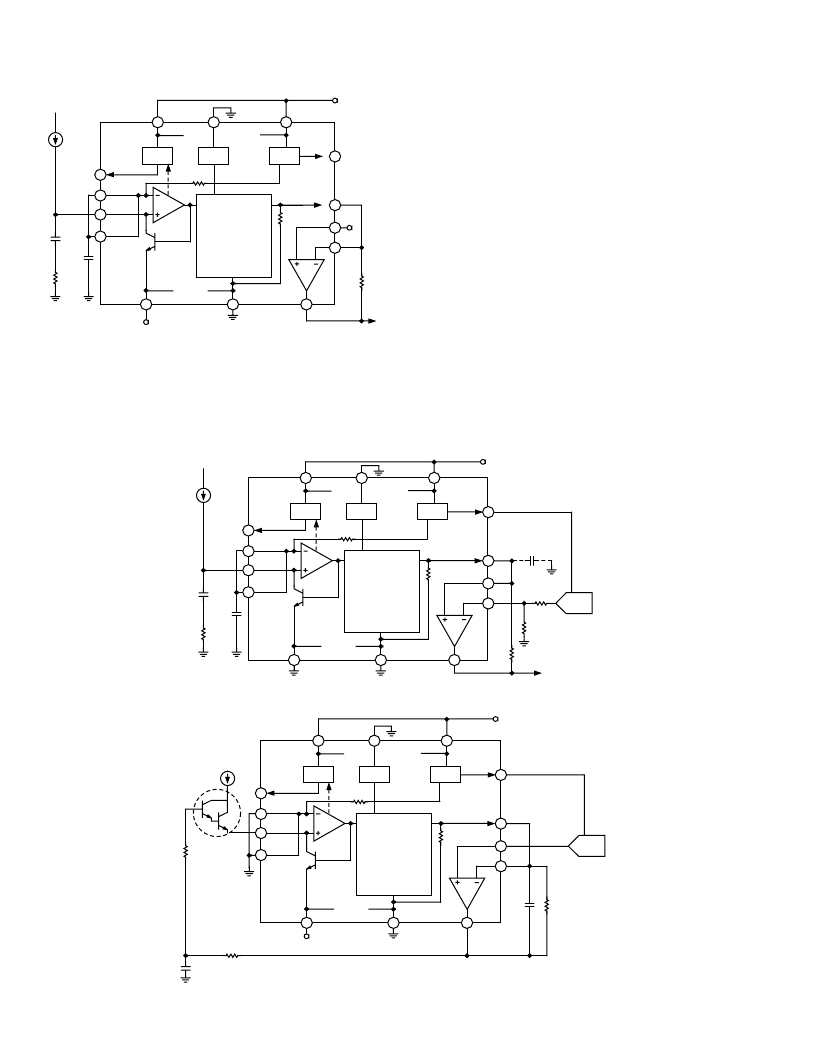
Figure 15. Using the Buffer to Invert the Polarity
of the Slope
When the gain is set to 13 (R
B
= 5 k
) the 2 V V
REF
can be tied
directly to BFIN, in which case the starting point for the output
response is at 4 V. However, since the slope in this case is only
–
0.2 V/decade, the full current range will only take the output
down by 1.6 V. Clearly, a higher slope (or gain) is desirable, in
which case V
OFS
should be set to a smaller voltage to avoid railing
the output at low currents. If V
OFS
= 1.2 V and G = 33, VOUT
now starts at 4.8 V and falls through this same voltage toward
ground with a slope of
–
0.6 V per decade, spanning the full
range of I
PD
.
Programmable Level Comparator with Hysteresis
The buffer amplifier and reference voltage permit a calibrated
level detector to be realized. Figure 16 shows the use of a 10-bit
MDAC to control the setpoint to within 0.1 dB of an exact value
over the 100 dB range of 1 nA
≤
I
PD
≤
100
μ
A when the full-
scale output of the MDAC is equal to that of its reference. The
2 V V
REF
also sets the minimum value of V
SPT
to 0.2 V, correspond-
ing to an input of 1 nA. Since 100 dB at the VLOG interface
corresponds to a 1 V span, the resistor network is calculated to
provide a maximum V
SPT
of 1.2 V while adding the required
10% of V
REF
.
In this example, the hysteresis range is arranged to be 0.1 dB,
(1 mV at VLOG) when using a 5 V supply. This will usually be
adequate to prevent noise that causes the comparator output to
thrash. That risk can be reduced further by using a low-pass filtering
capacitor at V
LOG
(shown dotted) to decrease the noise bandwidth.
6
3
4
PDB
BIAS
VREF
10
2
12
VPDB
VSUM
INPT
VSUM
5
1
VNEG
~10k
ACOM
14
VPS2
PWDN
VPS1
VREF
7
VLOG
8
BFIN
9
BFNG
TEMPERATURE
COMPENSATION
5k
11
VOUT
0.5V
I
PD
NC
750
1nF
13
V
P
NC = NO CONNECT
50M
V
OUT
10nF
V
SPT
VREF
VOUT
MDAC
49.9k
100k
RH
AD8304
Figure 16. Calibrated Level Comparator
6
3
4
PDB
BIAS
VREF
10
2
12
VPDB
VSUM
INPT
VSUM
5
1
VNEG
V
N
(–0.5V TO –5V)
~10k
ACOM
14
VPS2
PWDN
VPS1
VREF
7
VLOG
8
BFIN
9
BFNG
TEMPERATURE
COMPENSATION
5k
11
VOUT
0.5V
I
SRC
NC
25k
13
V
P
NC = NO CONNECT
C2
1nF
1k
VREF
VOUT
MDAC
C1
10nF
100k
AD8304
Figure 17. Multidecade Current Source
相關PDF資料 |
PDF描述 |
|---|---|
| AD8304ARU | 160 dB Range (100 pA -10 mA) Logarithmic Converter |
| AD8304ARU-REEL7 | 160 dB Range (100 pA -10 mA) Logarithmic Converter |
| AD8305 | 100 dB Range (10 nA to 1 mA) Logarithmic Converter |
| AD8305ACP | 100 dB Range (10 nA to 1 mA) Logarithmic Converter |
| AD8305ACP-REEL7 | 100 dB Range (10 nA to 1 mA) Logarithmic Converter |
相關代理商/技術參數 |
參數描述 |
|---|---|
| AD8304-EVALZ | 制造商:Analog Devices 功能描述:Evaluation Kit For 160 DB Range Logarithmic Converter 制造商:Analog Devices 功能描述:EVAL KIT FOR 160 DB RANGE (100 PA -10 MA) LOGARITHMIC CNVRTR - Bulk 制造商:Analog Devices 功能描述:EVAL LOGARITHMIC DECTECTOR AD8304 |
| AD8304XRU | 制造商:Analog Devices 功能描述: |
| AD8305 | 制造商:Analog Devices 功能描述:SP AMP LOG AMP SGL R-R O/P 6V/12V 16LFCSP EP - Bulk |
| AD8305_CSURF | 制造商:Analog Devices 功能描述: |
| AD8305ACP | 制造商:AD 制造商全稱:Analog Devices 功能描述:100 dB Range (10 nA to 1 mA) Logarithmic Converter |
發布緊急采購,3分鐘左右您將得到回復。