- 您現在的位置:買賣IC網 > PDF目錄373942 > AD8304 (Analog Devices, Inc.) 160 dB Range (100 pA -10 mA) Logarithmic Converter PDF資料下載
參數資料
| 型號: | AD8304 |
| 廠商: | Analog Devices, Inc. |
| 英文描述: | 160 dB Range (100 pA -10 mA) Logarithmic Converter |
| 中文描述: | 160分貝范圍(100功率放大器-10毫安)對數轉換器 |
| 文件頁數: | 11/20頁 |
| 文件大小: | 4286K |
| 代理商: | AD8304 |
REV. A
AD8304
–11–
In addition to uses in filter and comparator functions, the buffer
amplifier provides the means to adjust both the slope and inter-
cept, which require a minimal number of external components.
The high input impedance at BFIN, low input offset voltage,
large output swing, and wide bandwidth of this amplifier permit
numerous transformations of the basic V
LOG
signal, using stan-
dard op amp circuit practices. For example, it has been noted
that to raise the gain of the buffer, and therefore the slope, a
feedback attenuator, R
A
and R
B
in Figure 3, should be inserted
between VLOG and the inverting input Pin BFNG.
A wide range of gains may be used and the resistor magnitudes
are not critical; their parallel sum should be about equal to the
net source resistance at the noninverting input. When high gains
are used, the output dynamic range will be reduced; for maxi-
mum swing of 4.8 V, it will amount to simply 4.8 V/V
Y
decades.
Thus, using a ratio of 3 , to set up a slope 30 mV/dB (600 mV/
decade), eight decades can be handled, while with a ratio of 5 ,
which sets up a slope of 50 mV/dB (1 V/decade), the dynamic
range is 4.8 decades, or 96 dB. When using a lower positive
supply voltage, the calculation proceeds in the same way,
remembering to first subtract 0.2 V to allow for 0.1 V upper and
lower headroom in the output swing.
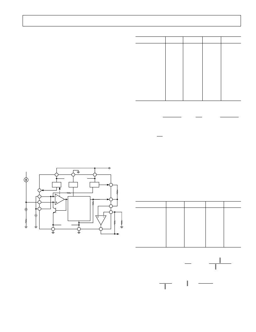
Alteration of the logarithmic intercept is only slightly more tricky.
First note that it will rarely be necessary to lower the intercept
below a value of 100 pA, since this merely raises all output volt-
ages further above ground. However, where this is required, the
first step is to raise the voltage V
LOG
by connecting a resistor, R
Z
,
from VLOG to VREF (2 V) as shown in Figure 4.
6
3
4
PDB
BIAS
VREF
10
2
12
VPDB
VSUM
INPT
VSUM
5
1
VNEG
~10k
ACOM
14
VPS2
PWDN
VPS1
VREF
7
VLOG
8
BFIN
9
BFNG
TEMPERATURE
COMPENSATION
5k
11
VOUT
0.5V
I
PD
NC
R1
750
10nF
C1
1nF
13
RA
V
P
V
OUT
NC = NO CONNECT
RB
RZ
Figure 4. Method for Lowering the Intercept
This has the effect of elevating V
LOG
for small inputs while lower-
ing the slope to some extent because of the shunt effect of R
Z
on the 5 k
output resistance. Then, if necessary, the slope may
be increased as before, using a feedback attenuator around the
buffer. Table II lists some examples of lowering the intercept
combined with various slope variations.
Table II. Examples of Lowering the Intercept
V
Y
(mV/decade)
200
200
200
300
300
300
400
400
400
500
500
500
I
Z
(pA)
1
10
50
1
10
50
1
10
50
1
10
50
R
A
(k )
20.0
10.0
3.01
10.0
8.06
6.65
11.5
9.76
8.66
16.5
14.3
13.0
R
B
(k )
100
100
100
12.4
12.4
12.4
8.2
8.2
8.2
8.2
8.2
8.2
R
Z
(k )
25
50
165
25
50
165
25
50
165
25
50
165
Equations for use with Table II:
where
V
G V
R
+
R
R
I
I
V
R
R
R
OUT
Y
Z
Z
LOG
PD
Z
REF
LOG
+
LOG
Z
=
×
×
+
×
log
10
G
R
R
R
k
A
B
LOG
= +
1
=
5
and
Generally, it will be useful to raise the intercept. Keep in mind
that this moves the V
LOG
line in Figure 2 to the right, lowering all
output values. Figure 5 shows how this is achieved. The feedback
resistors,
R
A
and
R
B
,
around the buffer are now augmented with
a third resistor,
R
Z
, placed between the Pins BFNG and VREF.
This raises the zero-signal voltage on BFNG, which has the effect
of pushing V
OUT
lower. Note that the addition of this resistor also
alters the feedback ratio. However, this is readily compensated
in the design of the network. Table III lists the resistor values
for representative intercepts.
Table III. Examples of Raising the Intercept
V
Y
(mV/decade)
300
300
400
400
400
500
500
500
I
Z
(nA)
10
100
10
100
500
10
100
500
R
A
(k )
7.5
8.25
10
9.76
9.76
12.4
12.4
11.5
R
B
(k )
37.4
130
16.5
25.5
36.5
12.4
16.5
20.0
R
C
(k )
24.9
18.2
25.5
16.2
13.3
24.9
16.5
12.4
Equations for use with Table III:
V
G V
I
I
V
R
R
R
R
R
OUT
Y
PD
Z
REF
A
B
A
B
C
=
×
×
+
log
–
10
where
G
R
R
R
R
R
R
R
R
R
A
B
C
A
B
A
B
A
B
= +
1
=
×
+
and
相關PDF資料 |
PDF描述 |
|---|---|
| AD8304-EVAL | 160 dB Range (100 pA -10 mA) Logarithmic Converter |
| AD8304ARU | 160 dB Range (100 pA -10 mA) Logarithmic Converter |
| AD8304ARU-REEL7 | 160 dB Range (100 pA -10 mA) Logarithmic Converter |
| AD8305 | 100 dB Range (10 nA to 1 mA) Logarithmic Converter |
| AD8305ACP | 100 dB Range (10 nA to 1 mA) Logarithmic Converter |
相關代理商/技術參數 |
參數描述 |
|---|---|
| AD8304ARU | 功能描述:IC LOGARITHM CONV 160DB 14-TSSOP RoHS:否 類別:集成電路 (IC) >> 線性 - 放大器 - 專用 系列:- 產品培訓模塊:Lead (SnPb) Finish for COTS Obsolescence Mitigation Program 標準包裝:60 系列:- 類型:可變增益放大器 應用:CATV 安裝類型:表面貼裝 封裝/外殼:20-WQFN 裸露焊盤 供應商設備封裝:20-TQFN-EP(5x5) 包裝:托盤 |
| AD8304ARU-REEL | 制造商:Analog Devices 功能描述:SP Amp LOG Amp Single R-R O/P 5.5V 14-Pin TSSOP T/R 制造商:Analog Devices 功能描述:SP AMP LOG AMP SGL R-R O/P 5.5V 14TSSOP - Tape and Reel |
| AD8304ARU-REEL7 | 功能描述:IC LOGARITHMIC CONV 14-TSSOP T/R RoHS:否 類別:集成電路 (IC) >> 線性 - 放大器 - 專用 系列:- 產品培訓模塊:Lead (SnPb) Finish for COTS Obsolescence Mitigation Program 標準包裝:60 系列:- 類型:可變增益放大器 應用:CATV 安裝類型:表面貼裝 封裝/外殼:20-WQFN 裸露焊盤 供應商設備封裝:20-TQFN-EP(5x5) 包裝:托盤 |
| AD8304ARUZ | 功能描述:IC LOGARITHM CONV 160DB 14-TSSOP RoHS:是 類別:集成電路 (IC) >> 線性 - 放大器 - 專用 系列:- 產品培訓模塊:Lead (SnPb) Finish for COTS Obsolescence Mitigation Program 標準包裝:60 系列:- 類型:可變增益放大器 應用:CATV 安裝類型:表面貼裝 封裝/外殼:20-WQFN 裸露焊盤 供應商設備封裝:20-TQFN-EP(5x5) 包裝:托盤 |
| AD8304ARUZ | 制造商:Analog Devices 功能描述:Logarithmic Amplifier IC |
發布緊急采購,3分鐘左右您將得到回復。