- 您現在的位置:買賣IC網 > PDF目錄373942 > AD8304 (Analog Devices, Inc.) 160 dB Range (100 pA -10 mA) Logarithmic Converter PDF資料下載
參數資料
| 型號: | AD8304 |
| 廠商: | Analog Devices, Inc. |
| 英文描述: | 160 dB Range (100 pA -10 mA) Logarithmic Converter |
| 中文描述: | 160分貝范圍(100功率放大器-10毫安)對數轉換器 |
| 文件頁數: | 9/20頁 |
| 文件大小: | 4286K |
| 代理商: | AD8304 |
REV. A
AD8304
–9–
To repeat the previous example: for a reference power level of
1 mW, a P
OPT
of 3 mW would correspond to a D
OPT
of 10 log
10
(3) =
4.77 dBm, while the equivalent intercept power of 110 pW will
correspond to a D
Z
of
–
69.6 dBm; now using Equation 8:
V
which is in agreement with the result from Equation 7.
mV
V
LOG
=
{
}
=
20
4 77
.
69. )
1 487
.
–
(
–
(9)
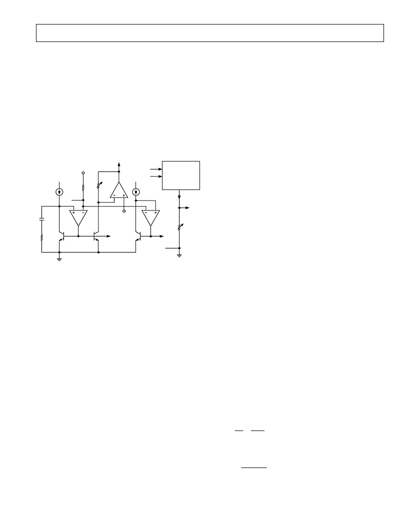
GENERAL STRUCTURE
The AD8304 addresses a wide variety of interfacing conditions
to meet the needs of fiber optic supervisory systems, and will also
be useful in many nonoptical applications. These notes explain
the structure of this unique translinear log amp. Figure 1 is a
simplified schematic showing the key elements.
PHOTODIODE
INPUT CURRENT
I
PD
INPT
~10k
C1
R1
VNEG (NORMALLY GROUNDED)
I
(INTERNAL)
0.5V
Q1
Q2
QM
INTERCEPT AND
TEMPERATURE
COMPENSATION
(SUBTRACT AND
DIVIDE BY T K)
VSUM
0.6V
0.5V
0.5V
V
BE1
V
BE2
200
V
PDB
VPDB
V
BE1
V
BE2–
296mVP
ACOM
VLOG
V
LOG
40 A/dec
5k
Figure 1. Simplified Schematic
The photodiode current I
PD
is received at input Pin INPT. The
summing voltage at this node is essentially equal to that on the
two adjacent guard pins, VSUM, due to the low offset voltage of
the ultralow bias J-FET op amp used to support the operation of
the transistor Q1, which converts the current to a logarithmic
voltage, as delineated in Equation 1. VSUM is needed to provide
the collector-emitter bias for Q1, and is internally set to 0.5 V,
using a quarter of the reference voltage of 2 V appearing on
Pin VREF.
In conventional translinear log amps, the summing node is gener-
ally
held at ground potential, but that condition is not
readily
realized in a single-supply part. To address this, the AD8304
also
supports the use of an optional negative supply voltage, V
N
, at
Pin VNEG. For a V
N
of at least
–
0.5 V the summing node can
be connected to ground potential. Larger negative voltages may
be used, with essentially no effect on scaling, up to a maximum
supply of 8 V between VPOS and VNEG. Note that the resistance
at the VSUM pins is approximately 10 k
to ground; this voltage
is not intended as a general bias source.
The input-dependent V
BE
of Q1 is compared with the fixed V
BE
of
a second transistor, Q2, which operates at an accurate internally
generated current, I
REF
= 10
μ
A. The overall intercept is arranged
to be 100,000 times smaller than
I
REF
, in later parts of the signal chain.
The difference between these two
V
BE
values can be written as
=
10
V
V
kT q
I
I
BE
BE
PD
REF
1
2
–
/ log
(
/
)
(10)
Thus, the uncertain and temperature-dependent saturation current,
I
S
that appears in Equation 1, has been eliminated. Next, to
eliminate the temperature variation of
kT/q
, this difference
voltage is applied to a processing block
—
essentially an analog divider
that effectively puts a variable proportional to temperature
underneath the
T
in Equation 10. In this same block,
I
REF
is trans-
formed to the much smaller current
I
Z
, to provide the previously
defined value for
V
LOG
, that is,
V
Recall that
V
Y
is 200 mV/decade and
I
Z
is 100 pA. Internally,
this is generated first as an output current of 40
μ
A/decade
(2
μ
A/dB) applied to an internal load resistor from VLOG to
ACOM that is laser-trimmed to 5 k
±
1%. The slope may be
altered at this point by adding an external shunt resistor. This is
required when using the minimum supply voltage of 3.0 V,
because the span of
V
LOG
for the full 160 dB (eight-decade)
range of
I
PD
amounts to 8
0.2 V = 1.6 V, which exceeds the
internal headroom at this node. Using a shunt of 5 k
, this is
reduced to 800 mV, that is, the slope becomes 5 mV/dB. In
those applications needing a higher slope, the buffer can provide
voltage gain. For example, to raise the output swing to 2.4 V,
which can be accommodated by the rail-to-rail buffer when
using a 3.0 V supply, a gain of 3 can be used which raises the
slope to 15 mV/dB. Slope variations implemented in these ways
do not affect the intercept. Keep in mind these measures to
address the limitations of a small positive supply voltage will not
be needed when
I
PD
is limited to about 1 mA maximum. They
can also be avoided by using a negative supply that allows
V
LOG
to run below ground, which will be discussed later.
Figure 1 shows how a sample of the input current is derived using
a very small monitoring transistor, Q
M
, connected in parallel with
Q1. This is used to generate the photodiode bias, V
PDB
, at Pin V
PDB
,
which varies from 0.6 V when I
PD
= 100 pA, and reverse-biases
the diode by 0.1 V (after subtracting the fixed 0.5 V at
INPT
)
and rises to 2.6 V at I
PD
= 10 mA, for a net diode bias of 2 V.
The driver for this output is current-limited to about 20 mA.
The system is completed by the final buffer amplifier, which is
essentially an uncommitted op amp with a rail-to-rail output
capability, a 10 MHz bandwidth, and good load-driving capabili-
ties, and may be used to implement multipole low-pass filters,
and a voltage reference for internal use in controlling the scaling,
but that is also made available at the 2.0 V level at Pin VREF.
Figure 2 shows the ideal output V
LOG
versus I
PD
.
Bandwidth and Noise Considerations
The response time and wide-band noise of translinear log amps
are fundamentally a function of the signal current
I
PD
. The
bandwidth becomes progressively lower as
I
PD
is reduced,
largely due to the effects of junction capacitances in Q1. This is
easily understood by noting that the transconductance (
g
m
) of a
bipolar transistor is a linear function of collector current, I
C
,
(hence, translinear), which in this case is just
I
PD
. The corre-
sponding incremental emitter resistance is:
kT
qI
PD
g
m
Basically, this resistance and the capacitance C
J
of the transistor
generate a time constant of r
e
C
J
and thus a corresponding low-pass
corner frequency of:
f
kTC
j
2
π
showing the proportionality of bandwidth to current.
V
I
I
LOG
Y
PD
Z
=
log (
/
)
(11)
r
e
=
=
1
(12)
qI
dB
PD
3
=
(13)
相關PDF資料 |
PDF描述 |
|---|---|
| AD8304-EVAL | 160 dB Range (100 pA -10 mA) Logarithmic Converter |
| AD8304ARU | 160 dB Range (100 pA -10 mA) Logarithmic Converter |
| AD8304ARU-REEL7 | 160 dB Range (100 pA -10 mA) Logarithmic Converter |
| AD8305 | 100 dB Range (10 nA to 1 mA) Logarithmic Converter |
| AD8305ACP | 100 dB Range (10 nA to 1 mA) Logarithmic Converter |
相關代理商/技術參數 |
參數描述 |
|---|---|
| AD8304ARU | 功能描述:IC LOGARITHM CONV 160DB 14-TSSOP RoHS:否 類別:集成電路 (IC) >> 線性 - 放大器 - 專用 系列:- 產品培訓模塊:Lead (SnPb) Finish for COTS Obsolescence Mitigation Program 標準包裝:60 系列:- 類型:可變增益放大器 應用:CATV 安裝類型:表面貼裝 封裝/外殼:20-WQFN 裸露焊盤 供應商設備封裝:20-TQFN-EP(5x5) 包裝:托盤 |
| AD8304ARU-REEL | 制造商:Analog Devices 功能描述:SP Amp LOG Amp Single R-R O/P 5.5V 14-Pin TSSOP T/R 制造商:Analog Devices 功能描述:SP AMP LOG AMP SGL R-R O/P 5.5V 14TSSOP - Tape and Reel |
| AD8304ARU-REEL7 | 功能描述:IC LOGARITHMIC CONV 14-TSSOP T/R RoHS:否 類別:集成電路 (IC) >> 線性 - 放大器 - 專用 系列:- 產品培訓模塊:Lead (SnPb) Finish for COTS Obsolescence Mitigation Program 標準包裝:60 系列:- 類型:可變增益放大器 應用:CATV 安裝類型:表面貼裝 封裝/外殼:20-WQFN 裸露焊盤 供應商設備封裝:20-TQFN-EP(5x5) 包裝:托盤 |
| AD8304ARUZ | 功能描述:IC LOGARITHM CONV 160DB 14-TSSOP RoHS:是 類別:集成電路 (IC) >> 線性 - 放大器 - 專用 系列:- 產品培訓模塊:Lead (SnPb) Finish for COTS Obsolescence Mitigation Program 標準包裝:60 系列:- 類型:可變增益放大器 應用:CATV 安裝類型:表面貼裝 封裝/外殼:20-WQFN 裸露焊盤 供應商設備封裝:20-TQFN-EP(5x5) 包裝:托盤 |
| AD8304ARUZ | 制造商:Analog Devices 功能描述:Logarithmic Amplifier IC |
發布緊急采購,3分鐘左右您將得到回復。