- 您現(xiàn)在的位置:買(mǎi)賣(mài)IC網(wǎng) > PDF目錄373942 > AD8304 (Analog Devices, Inc.) 160 dB Range (100 pA -10 mA) Logarithmic Converter PDF資料下載
參數(shù)資料
| 型號(hào): | AD8304 |
| 廠(chǎng)商: | Analog Devices, Inc. |
| 英文描述: | 160 dB Range (100 pA -10 mA) Logarithmic Converter |
| 中文描述: | 160分貝范圍(100功率放大器-10毫安)對(duì)數(shù)轉(zhuǎn)換器 |
| 文件頁(yè)數(shù): | 15/20頁(yè) |
| 文件大小: | 4286K |
| 代理商: | AD8304 |
第1頁(yè)第2頁(yè)第3頁(yè)第4頁(yè)第5頁(yè)第6頁(yè)第7頁(yè)第8頁(yè)第9頁(yè)第10頁(yè)第11頁(yè)第12頁(yè)第13頁(yè)第14頁(yè)當(dāng)前第15頁(yè)第16頁(yè)第17頁(yè)第18頁(yè)第19頁(yè)第20頁(yè)
REV. A
AD8304
–15–
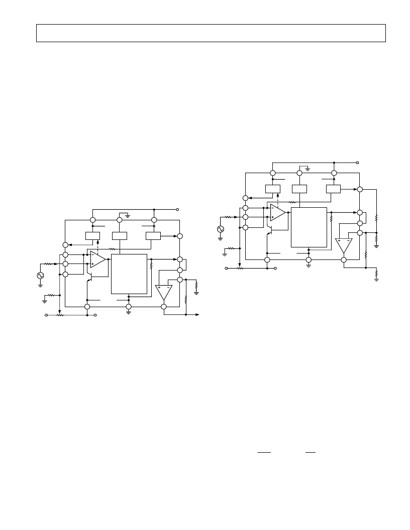
Summing Node at Ground and Voltage Inputs
A negative supply may be used to reposition the input node at
ground potential. A voltage as small as
–
0.5 V is sufficient. Figure13
shows the use of this feature. An input current of up to 10 mA is
supported.
This connection mode will be useful in cases where the source is a
positive voltage V
SIG
referenced to ground, rather than for use with
photodiodes, or other
“
perfect
”
current sources. R
IN
scales the
input current and should be chosen to optimally position the range
of I
PD
, or provide a very high input resistance, thus minimizing
the loading of the signal source. For example, assume a voltage
source that spans the four-decade range from 100 mV to 1 kV and
is desired to maximize R
IN
. When set to 1 G
, I
PD
spans the range
100 pA to 1 mA. Using a value of 10 M
, the same four decades
of input voltage would span the central current range of 10 nA
to 100 mA.
Smaller input voltages can be measured accurately when aided by
a small offset-nulling voltage applied to VSUM. The optional
network shown in Figure 13 provides more than
±
20 mV for
this purpose.
6
3
4
PDB
BIAS
VREF
10
2
12
VPDB
VSUM
INPT
VSUM
5
1
VNEG
~10k
ACOM
14
VPS2
PWDN
VPS1
VREF
7
VLOG
8
BFIN
9
BFNG
TEMPERATURE
COMPENSATION
5k
11
VOUT
0.5V
NC
13
V
P
NC = NO CONNECT
RB
RA
V
OUT
RIN
V
SIG
1k
10k
V
P
V
N
V
LOW
I
PD
AD8304
Figure 13. Using a Negative Supply and Placing VSUM at
Ground Permits Voltage-Mode Inputs
The minimum voltage that can be accurately measured is then
limited only by the drift in the input offset of the AD8304. The
specifications show the maximum spread over the full tempera-
ture and supply range. Over a limited temperature range, and with
a regulated supply, the offset drift will be lower; in this situation,
processing of inputs down to 5 mV is practicable.
The input system of the AD8304 is quasi-differential, so VSUM
can be placed at an arbitrary reference level V
LOW
, over a wide
range, and used as the
“
signal LO
”
of the source. For example,
using V
P
= 5 V and V
N
=
–
3 V, V
LOW
can be any voltage within
a
±
2.5 V range.
Providing Negative Outputs and Rescaling
As noted, the AD8304 allows the buffer to drive a load to negative
voltages with respect to ACOM, the analog common pin, which
is grounded. A negative supply capable of supporting the input
current I
PD
must be used, the fraction of quiescent bias that flows
out of the VNEG Pin, and the load current at VLOG. For the
example shown in Figure 14, this totals less than 20 mA when
driving a 1 k
load as far as
–
4 V.
The use of a much larger value for the intercept may be useful in
certain situations. In this example, it has been moved up four
decades, from the default value of 100 pA to the center of the full
eight-decade range at 1 mA. Using a voltage input as described
above, this corresponds to an altered voltage-mode intercept, V
Z
,
which would be 1 V for R
IN
= 1 M
. To take full advantage of the
larger output swing, the gain of the buffer has been increased to
4.53, resulting in a scaling of 900 mV/decade and a full-scale
output of
±
3.6 V.
6
3
4
PDB
BIAS
VREF
10
2
12
VPDB
VSUM
INPT
VSUM
5
1
VNEG
~10k
ACOM
14
VPS2
PWDN
VPS1
VREF
7
VLOG
8
BFIN
9
BFNG
TEMPERATURE
COMPENSATION
5k
11
VOUT
0.5V
NC
13
V
P
NC = NO CONNECT
RB
22.6k
RA
13.3k
V
OUT
RIN
V
SIG
1k
10k
V
P
V
N
V
LOW
I
PD
RL
1k
RC
12.4k
AD8304
Figure 14. Using a Negative Supply to Allow the
Output to Swing Below Ground
Inverting the Slope
The buffer is essentially an uncommitted op amp that can be used
to support the operation of the AD8304 in a variety of ways. It
can be completely disconnected from the signal chain when not
needed. Figure 15 shows its use as an inverting amplifier; this
changes the polarity of the slope. The output can either be
repositioned to all positive values by applying a fraction of V
REF
to the BFIN Pin, or range negative when using a negative supply.
The full design for a practical application is left undefined in this
brief illustration, but a few cases will be discussed.
For example, suppose we need a slope of
–
30 mV/dB; this requires
the gain to be three. Since V
LOG
exhibits a source resistance of
5 k
, R
B
must be 15 k
. In cases where a small negative supply
is available, the output voltage can swing below ground, and the
BFIN Pin may be grounded. But a negative slope is still possible
when only a single supply is used; a positive offset, V
OFS
, is applied
to this pin, as indicated in Figure 15. In general, the resulting
output voltage can be expressed as:
V
R
k
V
I
I
V
OUT
B
Y
PD
Z
OFS
=
×
+
–
log
5
10
(16)
相關(guān)PDF資料 |
PDF描述 |
|---|---|
| AD8304-EVAL | 160 dB Range (100 pA -10 mA) Logarithmic Converter |
| AD8304ARU | 160 dB Range (100 pA -10 mA) Logarithmic Converter |
| AD8304ARU-REEL7 | 160 dB Range (100 pA -10 mA) Logarithmic Converter |
| AD8305 | 100 dB Range (10 nA to 1 mA) Logarithmic Converter |
| AD8305ACP | 100 dB Range (10 nA to 1 mA) Logarithmic Converter |
相關(guān)代理商/技術(shù)參數(shù) |
參數(shù)描述 |
|---|---|
| AD8304ARU | 功能描述:IC LOGARITHM CONV 160DB 14-TSSOP RoHS:否 類(lèi)別:集成電路 (IC) >> 線(xiàn)性 - 放大器 - 專(zhuān)用 系列:- 產(chǎn)品培訓(xùn)模塊:Lead (SnPb) Finish for COTS Obsolescence Mitigation Program 標(biāo)準(zhǔn)包裝:60 系列:- 類(lèi)型:可變?cè)鲆娣糯笃?應(yīng)用:CATV 安裝類(lèi)型:表面貼裝 封裝/外殼:20-WQFN 裸露焊盤(pán) 供應(yīng)商設(shè)備封裝:20-TQFN-EP(5x5) 包裝:托盤(pán) |
| AD8304ARU-REEL | 制造商:Analog Devices 功能描述:SP Amp LOG Amp Single R-R O/P 5.5V 14-Pin TSSOP T/R 制造商:Analog Devices 功能描述:SP AMP LOG AMP SGL R-R O/P 5.5V 14TSSOP - Tape and Reel |
| AD8304ARU-REEL7 | 功能描述:IC LOGARITHMIC CONV 14-TSSOP T/R RoHS:否 類(lèi)別:集成電路 (IC) >> 線(xiàn)性 - 放大器 - 專(zhuān)用 系列:- 產(chǎn)品培訓(xùn)模塊:Lead (SnPb) Finish for COTS Obsolescence Mitigation Program 標(biāo)準(zhǔn)包裝:60 系列:- 類(lèi)型:可變?cè)鲆娣糯笃?應(yīng)用:CATV 安裝類(lèi)型:表面貼裝 封裝/外殼:20-WQFN 裸露焊盤(pán) 供應(yīng)商設(shè)備封裝:20-TQFN-EP(5x5) 包裝:托盤(pán) |
| AD8304ARUZ | 功能描述:IC LOGARITHM CONV 160DB 14-TSSOP RoHS:是 類(lèi)別:集成電路 (IC) >> 線(xiàn)性 - 放大器 - 專(zhuān)用 系列:- 產(chǎn)品培訓(xùn)模塊:Lead (SnPb) Finish for COTS Obsolescence Mitigation Program 標(biāo)準(zhǔn)包裝:60 系列:- 類(lèi)型:可變?cè)鲆娣糯笃?應(yīng)用:CATV 安裝類(lèi)型:表面貼裝 封裝/外殼:20-WQFN 裸露焊盤(pán) 供應(yīng)商設(shè)備封裝:20-TQFN-EP(5x5) 包裝:托盤(pán) |
| AD8304ARUZ | 制造商:Analog Devices 功能描述:Logarithmic Amplifier IC |
發(fā)布緊急采購(gòu),3分鐘左右您將得到回復(fù)。