- 您現在的位置:買賣IC網 > PDF目錄373942 > AD8304ARU (ANALOG DEVICES INC) 160 dB Range (100 pA -10 mA) Logarithmic Converter PDF資料下載
參數資料
| 型號: | AD8304ARU |
| 廠商: | ANALOG DEVICES INC |
| 元件分類: | 運動控制電子 |
| 英文描述: | 160 dB Range (100 pA -10 mA) Logarithmic Converter |
| 中文描述: | LOG OR ANTILOG AMPLIFIER, 10 MHz BAND WIDTH, PDSO14 |
| 封裝: | MO-153AB-1, TSSOP-14 |
| 文件頁數: | 10/20頁 |
| 文件大小: | 4286K |
| 代理商: | AD8304ARU |
REV. A
–10–
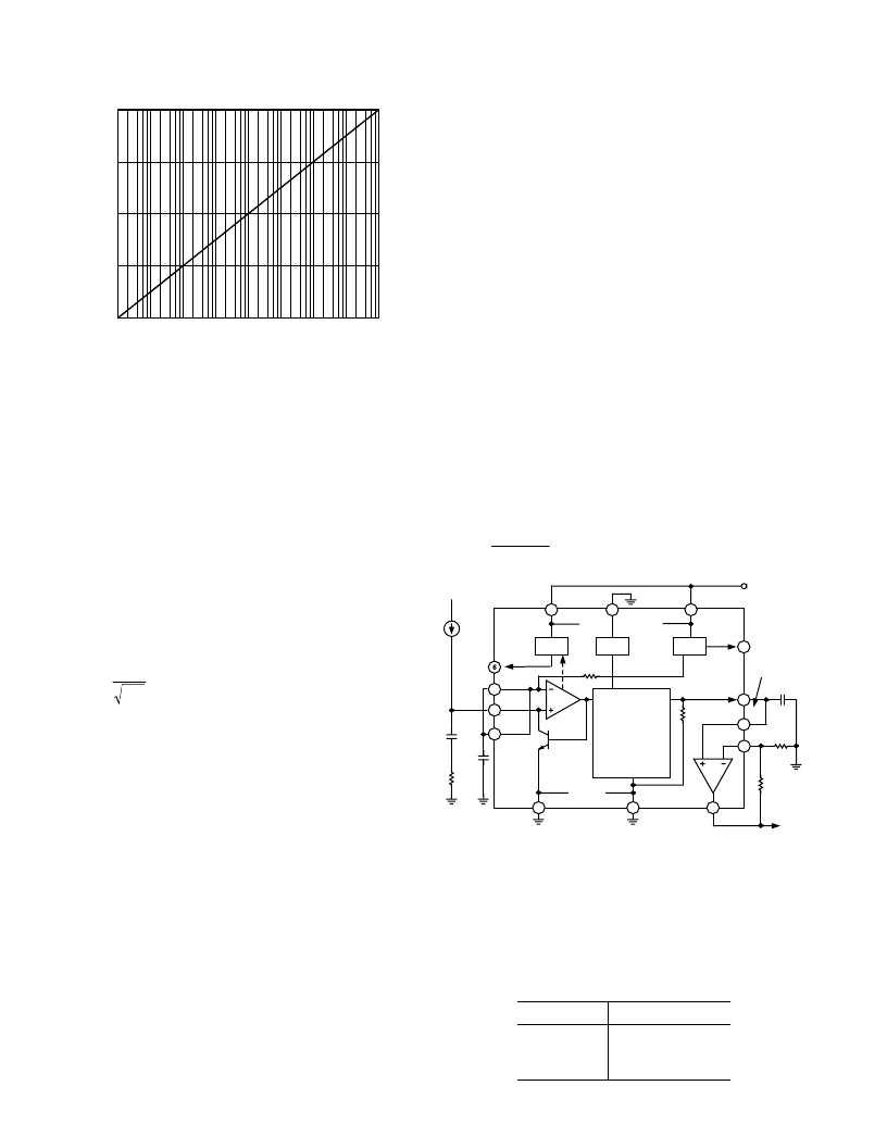
AD8304
INPUT – A
100p
10m
1n
10n
100n
1
10
100
1m
1.6
V
L
0.8
0
0.4
1.2
Figure 2. Ideal Form of V
LOG
vs. I
PD
Using a value of 0.3 pF for C
J
evaluates to 20 MHz/mA. There-
fore, the minimum bandwidth at I
PD
= 100 pA would be 2 kHz.
While this simple model is useful in making a point, it excludes
other effects that limit its usefulness. For example, the network
R1, C1 in Figure 1, which is necessary to stabilize the system over
the full range of currents, affects bandwidth at all values of I
PD
.
Later signal processing blocks also limit the maximum value.
TPC 7 shows ac response curves for the AD8304 at eight repre-
sentative currents of 100 pA to 10 mA, using R
1
= 750
and
C
1
= 1000 pF. The values for R1 and C1 ensure stability over
the full 160 dB dynamic range. More optimal values may be used
for smaller subranges. A certain amount of experimental trial and
error may be necessary to select the optimum input network
component values for a given application.
Turning now to the noise performance of a translinear log amp,
the relationship between
I
PD
and the voltage noise spectral density,
S
NSD
, associated with the V
BE
of Q1, evaluates to the following:
=
14 7
S
I
NSD
PD
(14)
where S
NSD
is nV/Hz, I
PD
is expressed in microamps and T
A
= 25
°
C.
For an input of 1 nA,
S
NSD
evaluates to almost 0.5
μ
V/
√
Hz; assum-
ing a 20 kHz bandwidth at this current, the integrated noise
voltage is 70
μ
V rms. However, the calculation is not complete.
The basic scaling of the V
BE
is approximately 3 mV/dB; translated
to 10 mV/dB, the noise predicted by Equation 14 must be multi-
plied by approximately 3.33. The additive noise effects associated
with the reference transistor, Q2, and the temperature compen-
sation circuitry must also be included. The final voltage noise
spectral density presented at the VLOG Pin varies inversely with
I
PD
, but not as simple as square root. TPC
S
8 and 9 show the
measured noise spectral density versus frequency at the VLOG
output, for the same nine-decade spaced values of
I
PD
.
Chip Enable
The AD8304 may be powered down by taking the PWDN Pin
to a high logic level. The residual supply current in the disabled
mode is typically 60
μ
A.
USING THE AD8304
The basic connections (Figure 3) include a 2.5:1 attenuator in
the feedback path around the buffer. This increases the basic slope
of 10 mV/dB at the VLOG Pin to 25 mV/dB at V
OUT
. For the
full dynamic range of 160 dB (80 dB optical), the output swing
is thus 4.0 V, which can be accommodated by the rail-to-rail
output stage when using the recommended 5 V supply.
The capacitor from VLOG to ground forms an optional single-
pole low-pass filter. Since the resistance at this pin is trimmed
to 5 k
, an accurate time constant can be realized. For ex-
ample, with C
FLT
= 10 nF, the
–
3 dB corner frequency is
3.2 kHz. Such filtering is useful in minimizing the output noise,
particularly when I
PD
is small. Multipole filters are more effec-
tive in reducing noise, and are discussed below. A capacitor
between VSUM and ground is essential for minimizing the
noise on this node. When the bias voltage at either VPDB or
VREF is not needed these pins should be left unconnected.
Slope and Intercept Adjustments
The choice of slope and intercept depends on the application.
The versatility of the AD8304 permits optimal choices to be
made in two common situations. First, it allows an input current
range of less than the full 160 dB to use the available voltage span
at the output. Second, it allows this output voltage range to be
optimally positioned to fit the input capacity of a subsequent
ADC. In special applications, very high slopes, such as 1 V/dec,
allow small subranges of I
PD
to be covered at high sensitivity.
The slope can be lowered without limit by the addition of a
shunt resistor, R
S
, from VLOG to ground. Since the resistance
at this pin is trimmed to 5 k
, the accuracy of the modified
slope will depend on the external resistor. It is calculated using:
V
V R
+
'
R
k
Y
S
S
=
5
(15)
3
4
PDB
BIAS
VREF
10
2
12
VPDB
VSUM
INPT
VSUM
5
1
VNEG
~10k
ACOM
14
VPS2
PWDN
VPS1
VREF
7
VLOG
8
BFIN
9
BFNG
TEMPERATURE
COMPENSATION
5k
11
VOUT
0.5V
I
PD
NC
R1
750
10nF
C1
1nF
13
RA
15k
RB
10k
CFLT
200mV/DEC
V
P
V
500mV/DEC
NC = NO CONNECT
Figure 3. Basic Connections (RA, RB, CFLT are
optional; R1 and C1 are the default values)
For example, using R
S
= 3 k
, the slope is lowered to 75 mV per
decade or 3.75 mV/dB. Table I provides a selection of suitable
values for R
S
and the resulting slopes.
Table I. Examples of Lowering the Slope
R
S
(k )
3
5
15
V
Y
(mV/dec)
75
100
150
相關PDF資料 |
PDF描述 |
|---|---|
| AD8304ARU-REEL7 | 160 dB Range (100 pA -10 mA) Logarithmic Converter |
| AD8305 | 100 dB Range (10 nA to 1 mA) Logarithmic Converter |
| AD8305ACP | 100 dB Range (10 nA to 1 mA) Logarithmic Converter |
| AD8305ACP-REEL7 | 100 dB Range (10 nA to 1 mA) Logarithmic Converter |
| AD8306 | 5 MHz-400 MHz 100 dB High Precision Limiting-Logarithmic Amplifier |
相關代理商/技術參數 |
參數描述 |
|---|---|
| AD8304ARU-REEL | 制造商:Analog Devices 功能描述:SP Amp LOG Amp Single R-R O/P 5.5V 14-Pin TSSOP T/R 制造商:Analog Devices 功能描述:SP AMP LOG AMP SGL R-R O/P 5.5V 14TSSOP - Tape and Reel |
| AD8304ARU-REEL7 | 功能描述:IC LOGARITHMIC CONV 14-TSSOP T/R RoHS:否 類別:集成電路 (IC) >> 線性 - 放大器 - 專用 系列:- 產品培訓模塊:Lead (SnPb) Finish for COTS Obsolescence Mitigation Program 標準包裝:60 系列:- 類型:可變增益放大器 應用:CATV 安裝類型:表面貼裝 封裝/外殼:20-WQFN 裸露焊盤 供應商設備封裝:20-TQFN-EP(5x5) 包裝:托盤 |
| AD8304ARUZ | 功能描述:IC LOGARITHM CONV 160DB 14-TSSOP RoHS:是 類別:集成電路 (IC) >> 線性 - 放大器 - 專用 系列:- 產品培訓模塊:Lead (SnPb) Finish for COTS Obsolescence Mitigation Program 標準包裝:60 系列:- 類型:可變增益放大器 應用:CATV 安裝類型:表面貼裝 封裝/外殼:20-WQFN 裸露焊盤 供應商設備封裝:20-TQFN-EP(5x5) 包裝:托盤 |
| AD8304ARUZ | 制造商:Analog Devices 功能描述:Logarithmic Amplifier IC |
| AD8304ARUZ-RL7 | 功能描述:IC LOGARITHM CONV 160DB 14-TSSOP RoHS:是 類別:集成電路 (IC) >> 線性 - 放大器 - 專用 系列:- 產品培訓模塊:Lead (SnPb) Finish for COTS Obsolescence Mitigation Program 標準包裝:60 系列:- 類型:可變增益放大器 應用:CATV 安裝類型:表面貼裝 封裝/外殼:20-WQFN 裸露焊盤 供應商設備封裝:20-TQFN-EP(5x5) 包裝:托盤 |
發(fā)布緊急采購,3分鐘左右您將得到回復。