- 您現在的位置:買賣IC網 > PDF目錄373942 > AD8306AR (ANALOG DEVICES INC) 5 MHz-400 MHz 100 dB High Precision Limiting-Logarithmic Amplifier PDF資料下載
參數資料
| 型號: | AD8306AR |
| 廠商: | ANALOG DEVICES INC |
| 元件分類: | 運動控制電子 |
| 英文描述: | 5 MHz-400 MHz 100 dB High Precision Limiting-Logarithmic Amplifier |
| 中文描述: | LOG OR ANTILOG AMPLIFIER, 395 MHz BAND WIDTH, PDSO16 |
| 封裝: | SO-16 |
| 文件頁數: | 11/16頁 |
| 文件大小: | 397K |
| 代理商: | AD8306AR |
REV. A
AD8306
–11–
1
2
3
4
5
6
7
8
VLOG
VPS2
PADL
LMHI
LMLO
PADL
FLTR
LMDR
COM2
VPS1
PADL
INHI
INLO
PADL
COM1
ENBL
AD8306
9
10
11
14
15
16
0.1
m
F
R2
10
V
NC
R
LIM
RSSI
0.1
m
F
R1
10
V
ENABLE
R
52.3
V
C1
0.01
m
F
SIGNAL
INPUTS
NC = NO CONNECT
12
13
V
S
(2.7V TO 6.5V)
C2
0.01
m
F
(SEE TEXT)
0.01
m
F
0.01
m
F
LIMITER
OUTPUT
R
LOAD
R
L
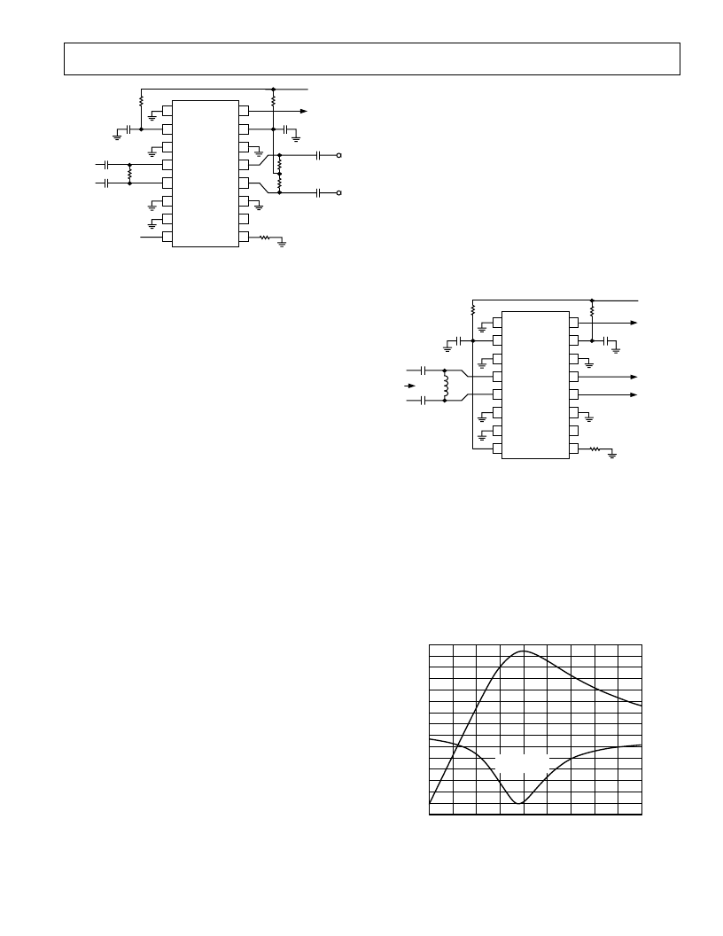
Figure 27. Basic Connections for Operating the Limiter
Depending on the application, the resulting voltage may be used
in a fully balanced or unbalanced manner. It is good practice to
retain both load resistors, even when only one output pin is
used. These should always be returned to the same well de-
coupled node on the PC board (see layout of evaluation board).
The unbalanced, or single-sided mode, is more inclined to result
in instabilities caused by the very high gain of the signal path.
The limiter current may be set as high as 10 mA (which requires
R
LIM
to be 40
) and can be optionally increased somewhat
beyond this level. It is generally inadvisable, however, to use a
high bias current, since the gain of this wide bandwidth signal
path is proportional to the bias current, and the risk of instabil-
ity is elevated as R
LIM
is reduced (recommended value is 400
).
However, as the size of R
LOAD
is increased, the bandwidth of the
limiter output decreases from 585 MHz for R
LOAD
= R
LIM
=
50
to 50 MHz for R
LOAD
= R
LIM
= 400
(bandwidth =
210 MHz for R
LOAD
= R
LIM
= 100
and 100 MHz for R
LOAD
=
R
LIM
= 200
). As a result, the minimum necessary limiter
output level should be chosen while maintaining the required
limiter bandwidth. For R
LIM
= R
LOAD
= 50
, the limiter output
is specified for input levels between –78 dBV (–65 dBm) and
+9 dBV (+22 dBm). The output of the limiter may be unstable
for levels below –78 dBV (–65 dBm). However, keeping R
LIM
above 100
will make instabilities on the output less likely for
input levels below –78 dBV.
A transformer or a balun (e.g., MACOM part number ETC1-1-13)
can be used to convert the differential limiter output voltages to
a single-ended signal.
Input Matching
Where either a higher sensitivity or a better high frequency
match is required, an input matching network is valuable. Using
a flux-coupled transformer to achieve the impedance transfor-
mation also eliminates the need for coupling capacitors, lowers
any dc offset voltages generated directly at the input, and use-
fully balances the drives to INHI and INLO, permitting full
utilization of the unusually large input voltage capacity of the
AD8306.
The choice of turns ratio will depend somewhat on the fre-
quency. At frequencies below 30 MHz, the reactance of the
input capacitance is much higher than the real part of the input
impedance. In this frequency range, a turns ratio of 2:9 will
lower the effective input impedance to 50
while raising the
input voltage by 13 dB. However, this does not lower the effect
of the short circuit noise voltage by the same factor, since there
will be a contribution from the input noise current. Thus, the
total noise
will be reduced by a smaller factor. The intercept at
the primary input will be lowered to –121 dBV (–108 dBm).
Impedance matching and drive balancing using a flux-coupled
transformer is useful whenever broadband coupling is required.
However, this may not always be convenient. At high frequen-
cies, it will often be preferable to use a narrow-band matching
network, as shown in Figure 28, which has several advantages.
First, the same voltage gain can be achieved, providing increased
sensitivity
, but now a measure of
selectively
is simultaneously
introduced. Second, the component count is low: two capacitors
and an inexpensive chip inductor are needed. Third, the net-
work also serves as a balun. Analysis of this network shows that
the amplitude of the voltages at INHI and INLO are quite simi-
lar when the impedance ratio is fairly high (i.e., 50
to 1000
).
1
2
3
4
5
6
7
8
VLOG
VPS2
PADL
LMHI
LMLO
PADL
FLTR
LMDR
COM2
VPS1
PADL
INHI
INLO
PADL
COM1
ENBL
AD8306
9
10
11
14
15
16
0.1
m
F
10
V
NC
R
LIM
RSSI
LIMITER
OUTPUT
0.1
m
F
10
V
C2 = C
M
Z
IN
NC = NO CONNECT
12
13
V
S
C1 = C
M
L
M
Figure 28. High Frequency Input Matching Network
Figure 29 shows the response for a center frequency of 100 MHz.
The response is down by 50 dB at one-tenth the center frequency,
falling by 40 dB per decade below this. The very high frequency
attenuation is relatively small, however, since in the limiting
case it is determined simply by the ratio of the AD8306’s input
capacitance to the coupling capacitors. Table I provides solu-
tions for a variety of center frequencies f
C
and matching from
impedances Z
IN
of nominally 50
and 100
. Exact values are
shown, and some judgment is needed in utilizing the nearest
standard values.
FREQUENCY – MHz
14
13
12
11
10
60
D
9
8
7
6
5
4
3
2
1
0
70
80
90
100
110
120
130
–1
140
150
GAIN
INPUT AT
TERMINATION
Figure 29. Response of 100 MHz Matching Network
相關PDF資料 |
PDF描述 |
|---|---|
| AD8306AR-REEL | 5 MHz-400 MHz 100 dB High Precision Limiting-Logarithmic Amplifier |
| AD8306AR-REEL7 | 5 MHz-400 MHz 100 dB High Precision Limiting-Logarithmic Amplifier |
| AD8307AN | Low Cost DC-500 MHz, 92 dB Logarithmic Amplifier |
| AD8307AR | Low Cost DC-500 MHz, 92 dB Logarithmic Amplifier |
| AD8307AR-REEL7 | Low Cost DC-500 MHz, 92 dB Logarithmic Amplifier |
相關代理商/技術參數 |
參數描述 |
|---|---|
| AD8306AR-REEL | 制造商:Analog Devices 功能描述:SP Amp LOG Amp Single 6.5V 16-Pin SOIC N T/R |
| AD8306AR-REEL7 | 功能描述:IC LOG-LIMITING AMP HP 16-SOIC RoHS:否 類別:集成電路 (IC) >> 線性 - 放大器 - 專用 系列:- 產品培訓模塊:Lead (SnPb) Finish for COTS Obsolescence Mitigation Program 標準包裝:60 系列:- 類型:可變增益放大器 應用:CATV 安裝類型:表面貼裝 封裝/外殼:20-WQFN 裸露焊盤 供應商設備封裝:20-TQFN-EP(5x5) 包裝:托盤 |
| AD8306ARZ | 功能描述:IC LOG-LIMITING AMP 16-SOIC RoHS:是 類別:集成電路 (IC) >> 線性 - 放大器 - 專用 系列:- 產品培訓模塊:Lead (SnPb) Finish for COTS Obsolescence Mitigation Program 標準包裝:60 系列:- 類型:可變增益放大器 應用:CATV 安裝類型:表面貼裝 封裝/外殼:20-WQFN 裸露焊盤 供應商設備封裝:20-TQFN-EP(5x5) 包裝:托盤 |
| AD8306ARZ | 制造商:Analog Devices 功能描述:Logarithmic Amplifier IC |
| AD8306ARZ-REEL | 制造商:Analog Devices 功能描述:SP Amp LOG Amp Single 6.5V 16-Pin SOIC N T/R 制造商:Analog Devices 功能描述:SP AMP LOG AMP SGL 6.5V 16SOIC N - Tape and Reel |
發布緊急采購,3分鐘左右您將得到回復。