- 您現在的位置:買賣IC網 > PDF目錄373942 > AD8307 (Analog Devices, Inc.) Low Cost DC-500 MHz, 92 dB Logarithmic Amplifier(對數放大器) PDF資料下載
參數資料
| 型號: | AD8307 |
| 廠商: | Analog Devices, Inc. |
| 元件分類: | 運動控制電子 |
| 英文描述: | Low Cost DC-500 MHz, 92 dB Logarithmic Amplifier(對數放大器) |
| 中文描述: | 低成本DC - 500兆赫,九十二分貝對數放大器(對數放大器) |
| 文件頁數: | 17/20頁 |
| 文件大小: | 303K |
| 代理商: | AD8307 |
AD8307
–17–
REV. 0
INPUT POWER – dBm
2.50
2.25
0
–100
20
V
O
–80
–20
0
2.00
1.25
1.00
0.50
WITH FILTER
–60
–40
ERROR
(WITH FILTER)
WITHOUT
FILTER
0.25
0.75
1.50
1.75
–2
–1
0
1
2
E
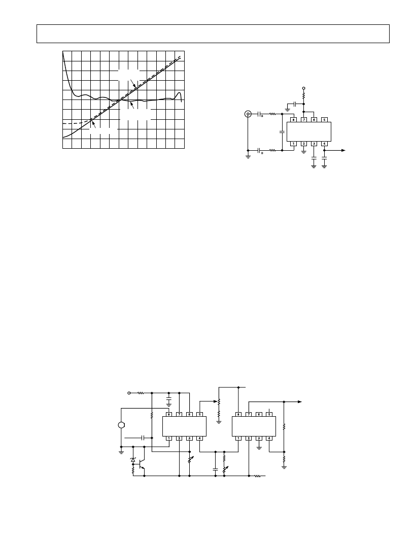
Figure 41. Results for 120 dB Measurement System
Operation at Low Frequencies
T he AD8307 provides excellent logarithmic conformance at
signal frequencies that may be arbitrarily low, depending only
on the values used for the input coupling capacitors. It may also
be desirable to add a low-pass input filter in order to desensitize
the log amp to HF signals. Figure 42 shows a simple arrange-
ment, providing coupling with an attenuation of 20 dB; the
intercept is shifted up by this attenuation, from –84 dBm to
–64 dBm, and the input range is now 0.5 mV to 20 V (sine
amplitude).
A high pass 3 dB corner frequency of nominally 3 Hz is set by
the 10
μ
F coupling capacitors C1 and C2, which are preferably
tantalum electrolytics (note the polarity) and a low pass 3 dB
corner frequency of 200 kHz (set by C3 and the effective resis-
tance at the input of 1 k
). T he –1% amplitude error points
occur at 20 Hz and 30 kHz. T hese are readily altered to suit
other applications by simple scaling. When C3 is zero, the low
pass corner is at 200 MHz. Note that the lower end of the dy-
namic range is improved by this capacitor, which provides es-
sentially an HF short circuit at the input, thus significantly
lowering the wideband noise; the noise reduction is about 2 dB
compared to the case when the AD8307 is driven from a 50
source.
T o ensure that the output is free of post-demodulation ripple, it
is necessary to lower the low-pass filter time-constant. T his is
provided by C5; with the value shown, the output time-constant
is 125 ms. (See also Figure 38 for a more elaborate filter). Finally,
to improve the law-conformance at very low signal levels and at
low frequencies, C4 has been added to the offset compensation
loop.
INP VPS ENB INT
AD8307
INM COM OFS OUT
+5V
C3
750pF
C2
10
m
F
C5
1
m
F
C1
10
m
F
0.1
m
F
NC
4.7
V
C4
1
m
F
V
25mV/dB
R2
5k
0.5mV
TO 20V
SINE
AMPLITUDE
FOR SLOPE AND
INTERCEPT ADJUSTMENTS
SEE FIGURE 35
R1
5k
V
IN
NC = NO CONNECT
Figure 42. Connections for Low Frequency Operation
DC-Coupled Applications
It may occasionally be necessary to provide response to dc in-
puts. Since the AD8307 is internally dc-coupled, there is no
fundamental reason why this is precluded. However, there is a
practical constraint, which is that its inputs must be positioned
about 2 V above the COM potential for proper biasing of the
first stage. If it happens that the source is a differential signal at
this level, it may be directly connected to the input. For ex-
ample, a microwave detector can be ac-coupled at its RF input
and its baseband load then automatically provided by the “float-
ing” R
IN
and C
IN
of the AD8307, at about V
P
/2.
Usually, the source will be a single-sided ground-referenced
signal, and it will thus be necessary to provide a negative supply
for the AD8307. T his can be achieved as shown in Figure 43.
T he output is now referenced to this negative supply, and it is
necessary to provide an output interface that performs a differ-
ential-to-single-sided conversion. T his is the purpose of the
AD830. T he slope may be arranged to be 20 mV/dB, when the
output ideally runs from zero, for a dc input of 10
μ
V, to +2.2 V
for an input of 4 V. T he AD8307 is fundamentally insensitive to
the sign of the input signal, but with this biasing scheme, the
maximum negative input is constrained to about –1.5 V. T he
transfer function after trimming and with R7 = 0, is
V
OUT
= (0.4
V
) log
10
(
V
IN
/10
μ
V)
INP VPS ENB INT
AD8307
INM COM OFS OUT
VP
INT
AD830
NC
VN
X1
X2
Y1
Y2
C1
0.1
m
F
C2
1
m
F
V
IN
TEMP
R2
3.3k
V
+5V
R1
4.7
V
VR2
50k
V
R5
*
* 51k
FOR
20mV/dB
5k FOR
100mV/dB
20mV/dB
+5V FOR 20mV/dB
+10V FOR 50mV/dB
+15V FOR 100mV/dB
V
OUT
R7
R8
R7,R8:
SEE TEXT
AD589
R3
1k
V
Q1
2N3904
VR1
2k
V
C3
0.1
m
F
–5V
NC = NO CONNECT
R6
32.4k
V
VR3
50k
V
R9
250
V
–5V
–2V
Figure 43. Connections for DC-Coupled Applications
相關PDF資料 |
PDF描述 |
|---|---|
| AD8309ARU-REEL | 5 MHz.500 MHz 100 dB Demodulating Logarithmic Amplifier with Limiter Output |
| AD8309-EVAL | 5 MHz.500 MHz 100 dB Demodulating Logarithmic Amplifier with Limiter Output |
| AD8309ARU | 5 MHz.500 MHz 100 dB Demodulating Logarithmic Amplifier with Limiter Output |
| AD8309ARU-REEL7 | 5 MHz.500 MHz 100 dB Demodulating Logarithmic Amplifier with Limiter Output |
| AD830 | High Speed, Video Difference Amplifier(高速,視頻差分運放) |
相關代理商/技術參數 |
參數描述 |
|---|---|
| AD8307_06 | 制造商:AD 制造商全稱:Analog Devices 功能描述:Low Cost DC-500 MHz, 92 dB Logarithmic Amplifier |
| AD8307AN | 功能描述:IC LOGARITHMIC AMP 8-DIP RoHS:否 類別:集成電路 (IC) >> 線性 - 放大器 - 專用 系列:- 產品培訓模塊:Lead (SnPb) Finish for COTS Obsolescence Mitigation Program 標準包裝:60 系列:- 類型:可變增益放大器 應用:CATV 安裝類型:表面貼裝 封裝/外殼:20-WQFN 裸露焊盤 供應商設備封裝:20-TQFN-EP(5x5) 包裝:托盤 |
| AD8307ANZ | 功能描述:IC LOGARITHMIC AMP 8-DIP RoHS:是 類別:集成電路 (IC) >> 線性 - 放大器 - 專用 系列:- 產品培訓模塊:Lead (SnPb) Finish for COTS Obsolescence Mitigation Program 標準包裝:60 系列:- 類型:可變增益放大器 應用:CATV 安裝類型:表面貼裝 封裝/外殼:20-WQFN 裸露焊盤 供應商設備封裝:20-TQFN-EP(5x5) 包裝:托盤 |
| AD8307AR | 功能描述:IC LOGARITHMIC AMP 92DB 8-SOIC RoHS:否 類別:集成電路 (IC) >> 線性 - 放大器 - 專用 系列:- 產品培訓模塊:Lead (SnPb) Finish for COTS Obsolescence Mitigation Program 標準包裝:60 系列:- 類型:可變增益放大器 應用:CATV 安裝類型:表面貼裝 封裝/外殼:20-WQFN 裸露焊盤 供應商設備封裝:20-TQFN-EP(5x5) 包裝:托盤 |
| AD8307AR-REEL | 功能描述:IC LOGARITHMIC AMP 8-SOIC T/R RoHS:否 類別:集成電路 (IC) >> 線性 - 放大器 - 專用 系列:- 產品培訓模塊:Lead (SnPb) Finish for COTS Obsolescence Mitigation Program 標準包裝:60 系列:- 類型:可變增益放大器 應用:CATV 安裝類型:表面貼裝 封裝/外殼:20-WQFN 裸露焊盤 供應商設備封裝:20-TQFN-EP(5x5) 包裝:托盤 |
發布緊急采購,3分鐘左右您將得到回復。