- 您現在的位置:買賣IC網 > PDF目錄373942 > AD8309-EVAL (Analog Devices, Inc.) 5 MHz.500 MHz 100 dB Demodulating Logarithmic Amplifier with Limiter Output PDF資料下載
參數資料
| 型號: | AD8309-EVAL |
| 廠商: | Analog Devices, Inc. |
| 元件分類: | 運動控制電子 |
| 英文描述: | 5 MHz.500 MHz 100 dB Demodulating Logarithmic Amplifier with Limiter Output |
| 中文描述: | 5 MHz.500兆赫和100分貝解調對數放大器輸出限幅 |
| 文件頁數: | 12/20頁 |
| 文件大小: | 311K |
| 代理商: | AD8309-EVAL |
REV. B
AD8309
–12–
A fully-programmable output interface is provided for the hard-
limited signal, permitting the user to establish the optimal output
current from its differential current-mode output. Its magnitude
is determined by the resistor R
LIM
placed between LMDR (Pin
9) and ground, across which a nominal bias voltage of ~400 mV
appears. Using R
LIM
= 200
, this dc bias current, which is
commutated alternately to the output pins, LMHI
and LMLO,
by the signal, is 2 mA. (The
total
supply current is somewhat
higher).
These currents may readily be converted to voltage form by the
inclusion of load resistors, which will typically range from a few
tens of ohms at 500 MHz to as high as 2 k
in lower frequency
applications. Alternatively, a resonant load may be used to ex-
tract the fundamental signal and modulation sidebands, mini-
mizing the out-of-band noise. A transformer or impedance
matching network may also be used at this output. The peak
voltage swing down from the supply voltage may be 1.2 V, be-
fore the output transistors go into saturation. (The Applications
section provides further information on the use of this interface).
The supply current for all sections except the limiter output
stage, and with no load attached to the RSSI output, is nomi-
nally 16 mA at T
A
= 27
°
C, substantially independent of supply
voltage. It varies in direct proportion to the absolute tempera-
ture (PTAT).
The RSSI load current is simply the voltage at
VLOG divided by the load resistance (e.g., 2.4 mA max in a
1 k
load). The limiter supply current is 1.1 times that flowing
in R
LIM
. The AD8309 may be enabled/disabled by a CMOS-
compatible level at ENBL (Pin 8).
In the following simplified interface diagrams, the components
denoted with an uppercase “R” are thin-film resistors having a
very low temperature-coefficient of resistance and high linearity
under large-signal conditions. Their absolute value is typically
within
±
20%. Capacitors denoted using an uppercase “C” have
a typical tolerance of
±
15% and essentially zero temperature or
voltage sensitivity. Most interfaces have additional small junc-
tion capacitances associated with them, due to active devices or
ESD protection; these may be neither accurate nor stable. Com-
ponent numbering in each of these interface diagrams is local.
Enable Interface
The chip-enable interface is shown in Figure 26. The current in
R1 controls the turn-on and turn-off states of the band-gap
reference and the bias generator, and is a maximum of 100
μ
A
when Pin 8 is taken to 5 V. Left unconnected, or at any voltage
below 1 V, the AD8309 will be disabled, when it consumes a
sleep current of much less than 1
μ
A (leakage currents only); when
tied to the supply, or any voltage above 2 V, it will be fully en-
abled. The internal bias circuitry requires approximately 300 ns
for either OFF or ON, while a delay of some 6
μ
s is required for
the supply current to fall below 10
μ
A.
1.3k
V
50k
V
4k
V
COMM
ENBL
R1
60k
V
TO BIAS
ENABLE
Figure 26. Enable Interface
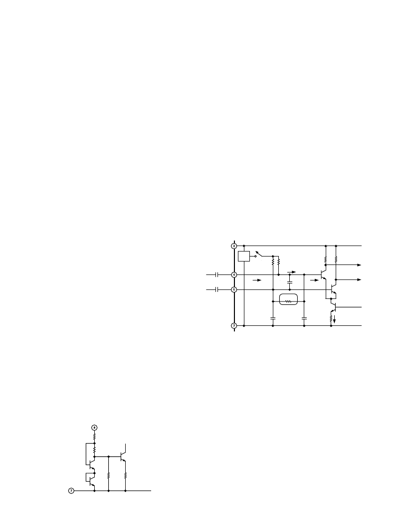
Input Interface
Figure 27 shows the essentials of the signal input interface. The
parasitic capacitances to ground are labeled C
P
; the differential
input capacitance, C
D
, mainly due to the diffusion capacitance
of Q1 and Q2. In most applications both input pins are ac-
coupled. The switch S closes when Enable is asserted. When
disabled, the inputs float, bias current I
E
is shut off, and the
coupling capacitors remain charged. If the log amp is disabled
for long periods, small leakage currents will discharge these
capacitors. If they are poorly matched, charging currents at
power-up can generate a transient input voltage which may
block the lower reaches of the dynamic range until it has be-
come much less than the signal.
In most applications, the input signal will be single-sided, and
may be applied to either Pin 4 or 5, with the remaining pin ac-
coupled to ground. Under these conditions, the largest input
signal that can be handled is –3 dBV (sine amplitude of 1 V)
when operating from a 3 V supply ; a +3 dBV input may be
handled using a supply of 4.5 V or greater. When using a fully-
balanced drive, the +3 dBV level may be achieved for the sup-
plies down to 2.7 V and +9 dBV using >4.5 V. For frequencies
in the range 10 MHz to 200 MHz these high drive levels are
easily achieved using a matching network (see
later). Using such
a network, having an inductor at the input, the input transient is
eliminated.
R
IN
= 1k
V
C
C
C
C
SIGNAL
INPUT
INLO
INHI
VPS1
COMM
1.78V
3.65k
V
3.65k
V
I
B
= 15mA
1.725V
1.725V
C
D
2.5pF
(TOP-END
DETECTORS)
2.6k
V
C
P
C
P
R
IN
= 3k
V
Q1
20e
Q2
20e
130
V
3.4mA
PTAT
GAIN BIAS
1.26V
67
V
67
V
TO STAGES
1 THRU 5
TO 2ND
STAGE
S
Figure 27. Signal Input Interface
Limiter Output Interface
The simplified limiter output stage is shown in Figure 28. The
bias for this stage is provided by a temperature-stable reference
voltage of nominally 400 mV which is forced across the external
resistor R
LIM
connected from Pin 9 (LMDR, or limiter drive) by
a special op amp buffer stage. The biasing scheme also intro-
duces a slight “lift” to this voltage to compensate for the finite
current gain of the current source Q3 and the output transistors
Q1 and Q2. A maximum current of 10 mA is permissible (R
LIM
= 40
). In special applications, it may be desirable to modulate
the bias current; an example of this is provided in the Applica-
tions section. Note that while the bias currents are temperature
stable, the ac gain of this stage will vary with temperature, by
–6 dB over a 120
°
C range.
A pair of supply and temperature stable complementary currents
is generated at the differential output LMHI and LMLO (Pins
12 and 13), having a square wave form with rise and fall times
of typically 0.4 ns, when load resistors of 50
are used. The
voltage at these output pins may swing to 1.2 V below the sup-
ply voltage applied to VPS2 (Pin 15).
相關PDF資料 |
PDF描述 |
|---|---|
| AD8309ARU | 5 MHz.500 MHz 100 dB Demodulating Logarithmic Amplifier with Limiter Output |
| AD8309ARU-REEL7 | 5 MHz.500 MHz 100 dB Demodulating Logarithmic Amplifier with Limiter Output |
| AD830 | High Speed, Video Difference Amplifier(高速,視頻差分運放) |
| AD8313ARM-REEL7 | 0.1 GHz-2.5 GHz, 70 dB Logarithmic Detector/Controller |
| AD8313ARM | 0.1 GHz-2.5 GHz, 70 dB Logarithmic Detector/Controller |
相關代理商/技術參數 |
參數描述 |
|---|---|
| AD8309-EVALZ | 制造商:Analog Devices 功能描述:EVAL KIT FOR 5 MHZ-500 MHZ 100DB DEMODULATING LOGARITHMIC AM - Bulk 制造商:Analog Devices 功能描述:EVAL BOARD, AD8309 LOGARITHMIC AMPLIFIER, Silicon Manufacturer:Analog Devices, Silicon Core Number:AD8309, Kit Application Type:RF / IF, Kit Contents:Eval Board AD8309, Features:(Not Applicable) |
| AD830AN | 制造商:Analog Devices 功能描述:Video Amp Single 85MHz 制造商:Analog Devices 功能描述:IC AMP DIFF VIDEO DIP8 830 |
| AD830ANZ | 功能描述:IC VIDEO DIFF AMP HS 8-DIP RoHS:是 類別:集成電路 (IC) >> 線性 - 放大器 - 視頻放大器和頻緩沖器 系列:- 標準包裝:1,000 系列:- 應用:驅動器 輸出類型:差分 電路數:3 -3db帶寬:350MHz 轉換速率:1000 V/µs 電流 - 電源:14.5mA 電流 - 輸出 / 通道:60mA 電壓 - 電源,單路/雙路(±):5 V ~ 12 V,±2.5 V ~ 6 V 安裝類型:表面貼裝 封裝/外殼:20-VFQFN 裸露焊盤 供應商設備封裝:20-QFN 裸露焊盤(4x4) 包裝:帶卷 (TR) |
| AD830AR | 功能描述:IC VIDEO DIFF AMP HS 8-SOIC RoHS:否 類別:集成電路 (IC) >> 線性 - 放大器 - 視頻放大器和頻緩沖器 系列:- 標準包裝:1,000 系列:- 應用:驅動器 輸出類型:差分 電路數:3 -3db帶寬:350MHz 轉換速率:1000 V/µs 電流 - 電源:14.5mA 電流 - 輸出 / 通道:60mA 電壓 - 電源,單路/雙路(±):5 V ~ 12 V,±2.5 V ~ 6 V 安裝類型:表面貼裝 封裝/外殼:20-VFQFN 裸露焊盤 供應商設備封裝:20-QFN 裸露焊盤(4x4) 包裝:帶卷 (TR) |
| AD830AR-REEL | 制造商:Analog Devices 功能描述:Video Amp Single 85MHz |
發布緊急采購,3分鐘左右您將得到回復。