- 您現(xiàn)在的位置:買(mǎi)賣(mài)IC網(wǎng) > PDF目錄373942 > AD8313ARM-REEL7 (ANALOG DEVICES INC) 0.1 GHz-2.5 GHz, 70 dB Logarithmic Detector/Controller PDF資料下載
參數(shù)資料
| 型號(hào): | AD8313ARM-REEL7 |
| 廠商: | ANALOG DEVICES INC |
| 元件分類: | 模擬信號(hào)調(diào)理 |
| 英文描述: | 0.1 GHz-2.5 GHz, 70 dB Logarithmic Detector/Controller |
| 中文描述: | SPECIALTY ANALOG CIRCUIT, PDSO8 |
| 封裝: | MO-187AA, MSOP-8 |
| 文件頁(yè)數(shù): | 10/16頁(yè) |
| 文件大小: | 261K |
| 代理商: | AD8313ARM-REEL7 |
第1頁(yè)第2頁(yè)第3頁(yè)第4頁(yè)第5頁(yè)第6頁(yè)第7頁(yè)第8頁(yè)第9頁(yè)當(dāng)前第10頁(yè)第11頁(yè)第12頁(yè)第13頁(yè)第14頁(yè)第15頁(yè)第16頁(yè)
AD8313
–10–
REV. B
Setpoint Interface, VSET
The setpoint interface is shown in Figure 26. The voltage V
SET
is divided by a factor of three in a resistive attenuator of total
resistance 18 k
. The signal is converted to a current by the
action of the op amp and the resistor R3 (1.5 k
), which bal-
ances the current generated by the summed output of the nine
detector cells at the input to the previous cell. The logarithmic
slope is nominally 3
×
4.0
μ
A/dB
×
1.5 k
≈
18 mV/dB.
VSET
VPOS
R1
12k
V
COMM
FDBK
TO O/P
STAGE
1
R2
6k
V
R3
1.5k
V
25
m
A
25
m
A
8
6
LP
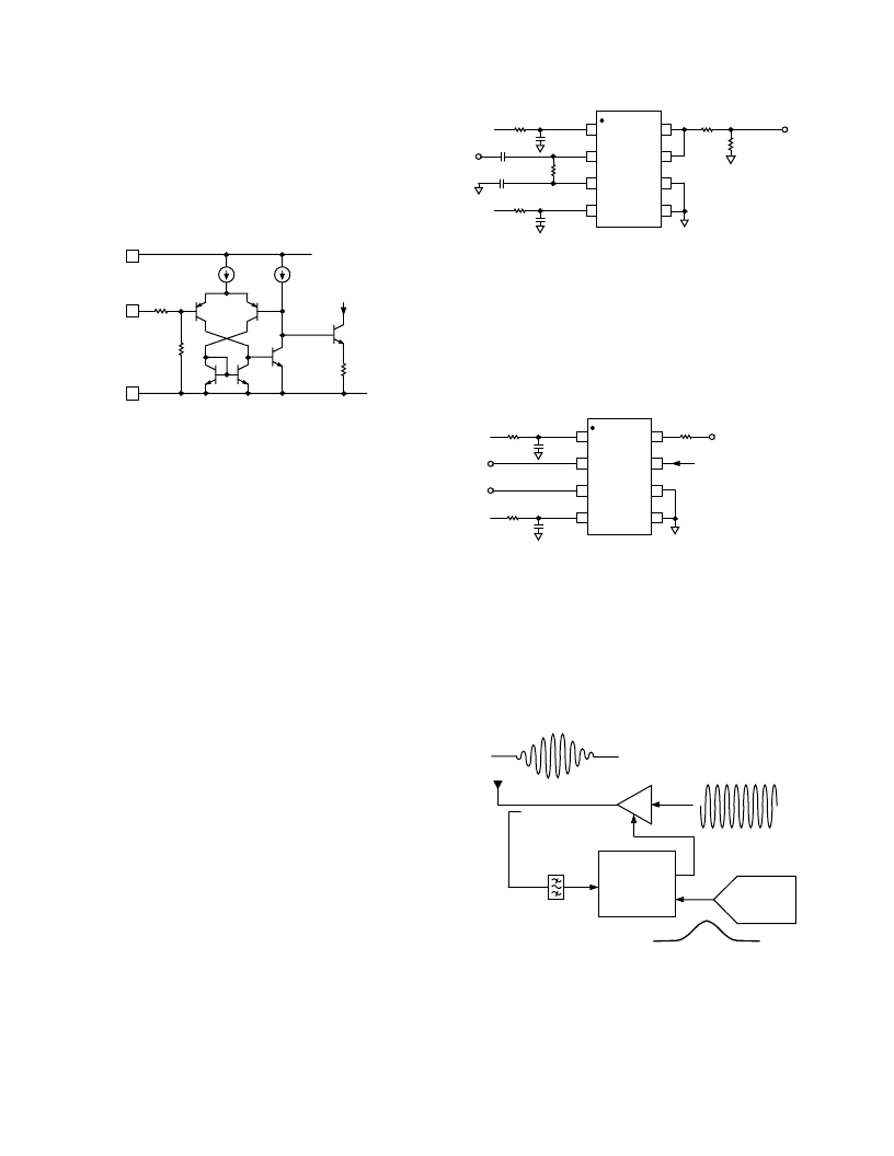
Figure 26. Setpoint Interface Circuitry
APPLICATIONS
Basic Connections for Log (RSSI) Mode
Figure 27 shows the AD8313 connected in its basic measure-
ment mode. A power supply of +2.7 V to +5.5 V is required.
The power supply to each of the VPOS pins should be decoupled
with a 0.1
μ
F, surface mount ceramic capacitor and a series
resistor of 10
.
The PWDN pin is shown as grounded. The AD8313 may be
disabled by a logic “HI” at this pin. When disabled, the chip
current is reduced to about 20
μ
A from its normal value of
13.7 mA. The logic threshold is at V
POS
/2 and the enable func-
tion occurs in about 1.8
μ
s; note, however, that further settling
time is generally needed at low input levels. While the input in
this case is terminated with a simple 50
broadband resistive
match, there are a wide variety of ways in which the input termi-
nation can be accomplished. These are discussed in the Input
Coupling section.
VSET is connected to VOUT to establish a feedback path that
controls the overall scaling of the logarithmic amplifier. The
load resistance, R
L
, should not be lower than 5 k
in order that
the full-scale output of 1.75 V can be generated with the limited
available current of 400
μ
A max.
As stated in the Absolute Maximum Ratings, an externally ap-
plied overvoltage on the VOUT pin that is outside the range 0 V
to V
POS
is sufficient to cause permanent damage to the device. If
overvoltages are expected on the VOUT pin, a series resistor
(R
PROT
) should be included as shown. A 500
resistor is suffi-
cient to protect against overvoltage up to
±
5 V; 1000
should
be used if an overvoltage of up to
±
15 V is expected. Since the
output stage is meant to drive loads of no more than 400
μ
A,
this resistor will not impact device performance for more high
impedance drive applications (higher output current applications
are discussed in the Increasing Output Current section).
R2
10
V
R
L
= 1M
V
0.1
m
F
53.6
V
680pF
680pF
R1
10
V
0.1
m
F
+V
S
+V
S
8
7
6
5
1
2
3
4
VPOS
AD8313
VOUT
INHI
INLO
VPOS PWDN
COMM
VSET
R
PROT
Figure 27. Basic Connections for Log (RSSI) Mode
Operating in the Controller Mode
Figure 28 shows the basic connections for operation in control-
ler mode. The link between VOUT and VSET is broken and a
“setpoint” is applied to VSET. Any difference between V
SET
and the equivalent input power to the AD8313, will drive V
OUT
either to the supply rail or close to ground. If V
SET
is greater
than the equivalent input power, V
OUT
will be driven towards
ground and vice versa.
V
INPUT
CONTROLLER
OUTPUT
R3
10
V
0.1
m
F
R1
10
V
0.1
m
F
+V
S
+V
S
8
7
6
5
1
2
3
4
VPOS
AD8313
VOUT
INHI
INLO
VPOS PWDN
COMM
VSET
R
PROT
Figure 28. Basic Connections for Operation in the
Controller Mode
This mode of operation is useful in applications where the out-
put power of an RF power amplifier (PA) is to be controlled by
an analog AGC loop (Figure 29). In this mode, a setpoint
voltage, proportional in dB to the desired output power, is ap-
plied to the VSET pin. A sample of the output power from the
PA, via a directional coupler or other means, is fed to the input
of the AD8313.
SETPOINT
CONTROL DAC
RFIN
VOUT
VSET
AD8313
DIRECTIONAL
COUPLER
POWER
AMPLIFIER
RF IN
ENVELOPE OF
TRANSMITTED
SIGNAL
Figure 29. Setpoint Controller Operation
V
OUT
is applied to the gain control terminal of the power ampli-
fier. The gain control transfer function of the power amplifier
should be an inverse relationship, i.e., increasing voltage de-
creases gain.
相關(guān)PDF資料 |
PDF描述 |
|---|---|
| AD8313ARM | 0.1 GHz-2.5 GHz, 70 dB Logarithmic Detector/Controller |
| AD8313ARM-REEL | 0.1 GHz-2.5 GHz, 70 dB Logarithmic Detector/Controller |
| AD8313-EVAL | 0.1 GHz-2.5 GHz, 70 dB Logarithmic Detector/Controller |
| AD8313 | 0.1 GHz-2.5 GHz,70dB Logarithmic Detector/Controller(頻率為0.1 GHz-2.5 GHz,增益為70dB的對(duì)數(shù)檢測(cè)器/控制器) |
| AD8314ARM | 100 MHz-2500 MHz 45 dB RF Detector/Controller |
相關(guān)代理商/技術(shù)參數(shù) |
參數(shù)描述 |
|---|---|
| AD8313ARMZ | 功能描述:IC LOGARTIHMIC AMP 70DB 8-MSOP RoHS:是 類別:RF/IF 和 RFID >> RF 檢測(cè)器 系列:- 產(chǎn)品變化通告:Product Discontinuation 15/May/2006 標(biāo)準(zhǔn)包裝:3,000 系列:- 頻率:100MHz ~ 2GHz RF 型:手機(jī),GSM,DCS,PCS 輸入范圍:- 精確度:- 電源電壓:2.7 V ~ 5.5 V 電流 - 電源:300µA 包裝:帶卷 (TR) 封裝/外殼:SC-74,SOT-457 其它名稱:NCS5000SNT1GOS |
| AD8313ARMZ | 制造商:Analog Devices 功能描述:IC DETECTOR/CONTROLLER 制造商:Analog Devices 功能描述:IC, DETECTOR/CONTROLLER |
| AD8313ARMZ | 制造商:Analog Devices 功能描述:IC, RF LOG DET, 100kHz to 2.5GHz, MSOP-8 |
| AD8313ARMZ-REEL | 功能描述:IC LOG DETECTOR/CTRLR 8MSOP RoHS:是 類別:RF/IF 和 RFID >> RF 檢測(cè)器 系列:- 產(chǎn)品變化通告:Product Discontinuation 15/May/2006 標(biāo)準(zhǔn)包裝:3,000 系列:- 頻率:100MHz ~ 2GHz RF 型:手機(jī),GSM,DCS,PCS 輸入范圍:- 精確度:- 電源電壓:2.7 V ~ 5.5 V 電流 - 電源:300µA 包裝:帶卷 (TR) 封裝/外殼:SC-74,SOT-457 其它名稱:NCS5000SNT1GOS |
| AD8313ARMZ-REEL7 | 功能描述:IC LOG DETECTOR/CTRLR 8-MSOP TR RoHS:是 類別:RF/IF 和 RFID >> RF 檢測(cè)器 系列:- 產(chǎn)品變化通告:Product Discontinuation 15/May/2006 標(biāo)準(zhǔn)包裝:3,000 系列:- 頻率:100MHz ~ 2GHz RF 型:手機(jī),GSM,DCS,PCS 輸入范圍:- 精確度:- 電源電壓:2.7 V ~ 5.5 V 電流 - 電源:300µA 包裝:帶卷 (TR) 封裝/外殼:SC-74,SOT-457 其它名稱:NCS5000SNT1GOS |
發(fā)布緊急采購(gòu),3分鐘左右您將得到回復(fù)。