- 您現在的位置:買賣IC網 > PDF目錄373945 > AD8383ACPZ (ANALOG DEVICES INC) Low Cost 10-Bit, 6-Channel Output Decimating LCD DecDriver PDF資料下載
參數資料
| 型號: | AD8383ACPZ |
| 廠商: | ANALOG DEVICES INC |
| 元件分類: | 顯示驅動器 |
| 英文描述: | Low Cost 10-Bit, 6-Channel Output Decimating LCD DecDriver |
| 中文描述: | LIQUID CRYSTAL DISPLAY DRIVER, QCC48 |
| 封裝: | 7 X 7 MM, 0.85 MM HEIGHT, MO-220VKKD-2, LFCSP-48 |
| 文件頁數: | 10/16頁 |
| 文件大小: | 376K |
| 代理商: | AD8383ACPZ |
AD8383
PCB DESIGN FOR GOOD THERMAL PERFORMANCE
The total maximum power dissipation of the AD8383 is partly
dependent on load. In a 6-channel 60 Hz XGA system running
at a 65 MHz clock rate, the total maximum power dissipation is
1.08 W at an LCD panel input capacitance of 150 pF.
Rev. 0 | Page 10 of 16
At the maximum specified clock rate of 100 Ms/s, the total
maximum power dissipation can exceed 2 W for large capacitive
loads, as shown in Table 4.
Although the maximum safe operating junction temperature is
higher, the AD8383 is 100% tested at a junction temperature of
125°C. Consequently, the maximum guaranteed operating
junction temperature is 125°C. To limit the maximum junction
temperature at or below the guaranteed maximum, the package,
in conjunction with the PCB, must effectively conduct heat
away from the junction.
The AD8383’s LFCSP package is designed to provide superior
thermal characteristics, partly achieved by an exposed die
paddle on the bottom surface of the package. In order to take
full advantage of this feature, the exposed paddle must be in
direct thermal contact with the PCB, which then serves as a
heat sink.
A thermally effective PCB must incorporate a thermal pad and
a thermal via structure. The thermal pad provides a solderable
contact surface on the top surface of the PCB. The thermal via
structure provides a thermal path to the inner and bottom
layers of the PCB to remove heat.
THERMAL PAD DESIGN
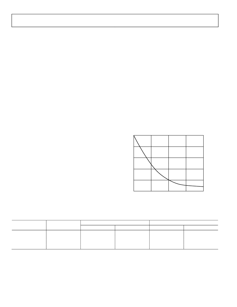
Thermal performance of the AD8383 varies logarithmically
with the contact area between the exposed thermal paddle and
the thermal pad on the top layer of the PCB. See Figure 11.
The θ
JA
(of the AD8383 mounted on a standard JEDEC PCB) is
reduced by approximately 40% as the contact area increases
from 0% (no thermal pad) to 50%. It approaches its specified
value as the contact area (on the JEDEC standard PCB)
approaches 100%.
In order to minimize thermal performance degradation of
production PCBs, the contact area between the thermal pad and
the PCB should be maximized. Therefore, the size of the
thermal pad should match the exposed 5.25 mm × 5.25 mm
paddle size. However, if the PCB design rules require a pad-to-
pad clearance of more than 0.3 mm, the size of the thermal pad
may be reduced to 5 mm × 5 mm. Additionally, a second
thermal pad of the same size should be placed on the bottom
side of the PCB. At least one thermal pad should be in direct
thermal (and electrical) contact with the AVCC plane.
25
30
35
40
45
50
θ
J
CONTACT AREA (%)
25
0
50
75
100
0
Figure 11. Thermal Performance vs. Contact Area (on a JEDEC PCB)
Table 4. Power Dissipation vs. Load Capacitance and VFS at 100 Ms/s Clock Rate
C
LOAD
(pF)
P
QUIESCENT
(W)
150
0.7
200
0.7
250
0.7
300
0.7
VFS = 5 V
VFS = 4 V
P
DYNAMIC
(W)
0.72
0.96
1.20
1.44
P
TOTAL
(W)
1.42
1.66
1.90
2.14
P
DYNAMIC
(W)
0.58
0.77
0.96
1.15
P
TOTAL
(W)
1.28
1.47
1.66
1.85
相關PDF資料 |
PDF描述 |
|---|---|
| AD8391 | xDSL Line Driver 3 V to 12 V with Power-Down |
| AD8391AR | xDSL Line Driver 3 V to 12 V with Power-Down |
| AD8391AR-EVAL | xDSL Line Driver 3 V to 12 V with Power-Down |
| AD8391AR-REEL | xDSL Line Driver 3 V to 12 V with Power-Down |
| AD8391AR-REEL7 | xDSL Line Driver 3 V to 12 V with Power-Down |
相關代理商/技術參數 |
參數描述 |
|---|---|
| AD8384 | 制造商:AD 制造商全稱:Analog Devices 功能描述:10-Bit, 6-Channel Decimating LCD DecDriver-R with Level Shifters |
| AD8384ASVZ | 功能描述:IC DRIVER LCD 6CH 10BIT 80-TQFP RoHS:是 類別:集成電路 (IC) >> PMIC - 顯示器驅動器 系列:DecDriver™ 產品培訓模塊:Lead (SnPb) Finish for COTS Obsolescence Mitigation Program 標準包裝:2,500 系列:- 顯示器類型:真空熒光 (VF) 配置:5 x 7(矩陣) 接口:串行 數字或字符:- 電流 - 電源:3.5mA 電源電壓:2.7 V ~ 3.6 V 工作溫度:-40°C ~ 125°C 安裝類型:表面貼裝 封裝/外殼:16-SSOP(0.154",3.90mm 寬) 供應商設備封裝:16-QSOP 包裝:帶卷 (TR) |
| AD8385 | 制造商:AD 制造商全稱:Analog Devices 功能描述:10-Bit, 12-Channel Decimating LCD DECDRIVER with Level Shifters |
| AD8385ASVZ | 制造商:Analog Devices 功能描述: |
| AD8386 | 制造商:AD 制造商全稱:Analog Devices 功能描述:10-Bit, 12-Channel Output Decimating LCD Driver |
發布緊急采購,3分鐘左右您將得到回復。