- 您現(xiàn)在的位置:買賣IC網(wǎng) > PDF目錄373945 > AD8383ACPZ (ANALOG DEVICES INC) Low Cost 10-Bit, 6-Channel Output Decimating LCD DecDriver PDF資料下載
參數(shù)資料
| 型號: | AD8383ACPZ |
| 廠商: | ANALOG DEVICES INC |
| 元件分類: | 顯示驅(qū)動器 |
| 英文描述: | Low Cost 10-Bit, 6-Channel Output Decimating LCD DecDriver |
| 中文描述: | LIQUID CRYSTAL DISPLAY DRIVER, QCC48 |
| 封裝: | 7 X 7 MM, 0.85 MM HEIGHT, MO-220VKKD-2, LFCSP-48 |
| 文件頁數(shù): | 13/16頁 |
| 文件大小: | 376K |
| 代理商: | AD8383ACPZ |
AD8383
Rev. 0 | Page 13 of 16
P
P
P
C
P
PCB
θ
PCB
θ
JC
T
CASE
T
PCB
θ
AIR-PCB
θ
AIR-CASE
T
A
T
J
0
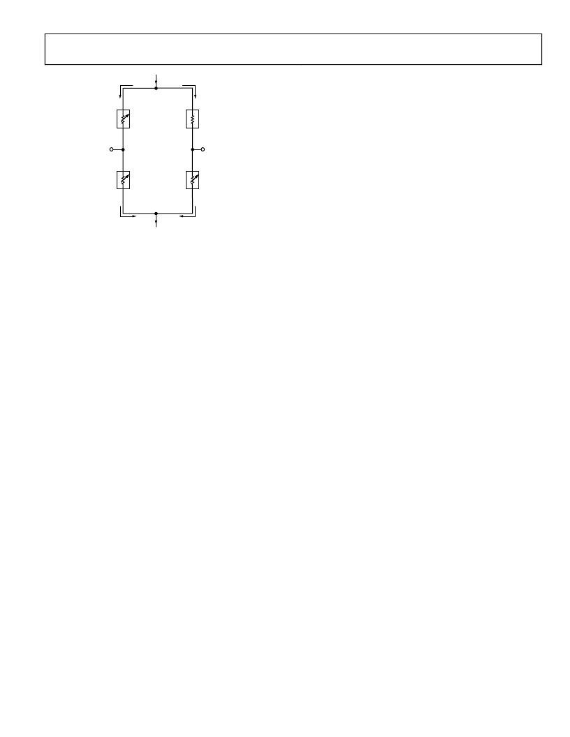
Figure 15. Simplified Thermal Equivalent Circuit
Verification of the Maximum Operating Junction
Temperature
In order to verify the system thermal design for compliance
with the maximum operating junction temperature specifica-
tion, temperature measurements T
CASE
and T
PCB
are required at
the maximum possible total power dissipation in a complete,
fully assembled LCD projection system.
Maximum possible total power dissipation of the AD8383
occurs when the video input to the projector is a pattern with
1-pixel-wide white and black vertical lines. An alternative
pattern that results in the maximum possible total power
dissipation is a 1-pixel checkerboard pattern. The expected total
power dissipation of the AD8383 in a 60 Hz, 6-channel XGA
projector displaying the 1-pixel-wide vertical line or checker-
board pattern is 1.08 W (at AVCC = 15.5 V, VCOM = 7 V, and
LCD capacitance = 150 pF).
Although the case and PCB temperatures are highly dependent
on the PCB design, their measured values are expected to be
similar at approximately 40°C above the ambient (on a typical
PCB with a minimal airflow whose thermal design follows the
recommendations described in this note). The junction temper-
ature then calculates to approximately 10°C above the case and
PCB temperatures. At a 70°C ambient temperature, the junction
temperature is expected to be at approximately 120°C.
The AD8383 has a relatively small thermal mass. In order to
minimize measurement errors due to the thermal mass of the
measuring device, a small-gauge thermocouple or a thermal
probe with a very small thermal mass is required for the mea-
surement of T
CASE
and T
PCB
.
Power-Up and Power-Down Sequencing
As indicated in the Absolute Maximum Ratings, the voltage at
any input pin cannot exceed its supply voltage by more than
0.5 V. To ensure compliance with the Absolute Maximum
Ratings, power-up and power-down sequencing may be
required.
During power-up, initial application of nonzero voltages to any
of the input pins must be delayed until the supply voltage ramps
up to at least the highest maximum operational input voltage.
During power-down, the voltage at any input pin must reach
zero during a period not exceeding the hold-up time of the
power supply.
Failure to comply with the Absolute Maximum Ratings may
result in functional failure or damage to the internal ESD
diodes.
Damaged ESD diodes may cause temporary parametric failures,
which may result in image artifacts. Damaged ESD diodes
cannot provide full ESD protection, thus reducing reliability.
The recommended sequence is
Power ON
1.
Apply power to supplies.
2.
Apply power to other I/Os.
Power OFF
1.
Remove power from I/Os.
2.
VBIAS Generation—V1, V2 Input Pin Functionality
In order to avoid image flicker, a bias voltage of approximately
1 V minimum must be maintained across the pixels of HTPS
LCDs. The AD8383 provides two methods of maintaining this
bias voltage.
Internal Bias Voltage Generation
Standard systems that internally generate the bias voltage
reserve the upper-most code range for the bias voltage and use
the remaining code range to encode the video for gamma
correction.
Remove power from supplies.
相關(guān)PDF資料 |
PDF描述 |
|---|---|
| AD8391 | xDSL Line Driver 3 V to 12 V with Power-Down |
| AD8391AR | xDSL Line Driver 3 V to 12 V with Power-Down |
| AD8391AR-EVAL | xDSL Line Driver 3 V to 12 V with Power-Down |
| AD8391AR-REEL | xDSL Line Driver 3 V to 12 V with Power-Down |
| AD8391AR-REEL7 | xDSL Line Driver 3 V to 12 V with Power-Down |
相關(guān)代理商/技術(shù)參數(shù) |
參數(shù)描述 |
|---|---|
| AD8384 | 制造商:AD 制造商全稱:Analog Devices 功能描述:10-Bit, 6-Channel Decimating LCD DecDriver-R with Level Shifters |
| AD8384ASVZ | 功能描述:IC DRIVER LCD 6CH 10BIT 80-TQFP RoHS:是 類別:集成電路 (IC) >> PMIC - 顯示器驅(qū)動器 系列:DecDriver™ 產(chǎn)品培訓(xùn)模塊:Lead (SnPb) Finish for COTS Obsolescence Mitigation Program 標準包裝:2,500 系列:- 顯示器類型:真空熒光 (VF) 配置:5 x 7(矩陣) 接口:串行 數(shù)字或字符:- 電流 - 電源:3.5mA 電源電壓:2.7 V ~ 3.6 V 工作溫度:-40°C ~ 125°C 安裝類型:表面貼裝 封裝/外殼:16-SSOP(0.154",3.90mm 寬) 供應(yīng)商設(shè)備封裝:16-QSOP 包裝:帶卷 (TR) |
| AD8385 | 制造商:AD 制造商全稱:Analog Devices 功能描述:10-Bit, 12-Channel Decimating LCD DECDRIVER with Level Shifters |
| AD8385ASVZ | 制造商:Analog Devices 功能描述: |
| AD8386 | 制造商:AD 制造商全稱:Analog Devices 功能描述:10-Bit, 12-Channel Output Decimating LCD Driver |
發(fā)布緊急采購,3分鐘左右您將得到回復(fù)。