- 您現在的位置:買賣IC網 > PDF目錄373946 > AD8401 (Analog Devices, Inc.) 8-Bit, 4-Channel Data Acquisition System(8位4通道DAS) PDF資料下載
參數資料
| 型號: | AD8401 |
| 廠商: | Analog Devices, Inc. |
| 英文描述: | 8-Bit, 4-Channel Data Acquisition System(8位4通道DAS) |
| 中文描述: | 8位,4通道數據采集系統(4通道8位DAS)的 |
| 文件頁數: | 5/12頁 |
| 文件大小: | 182K |
| 代理商: | AD8401 |
AD8401
–5–
REV. 0
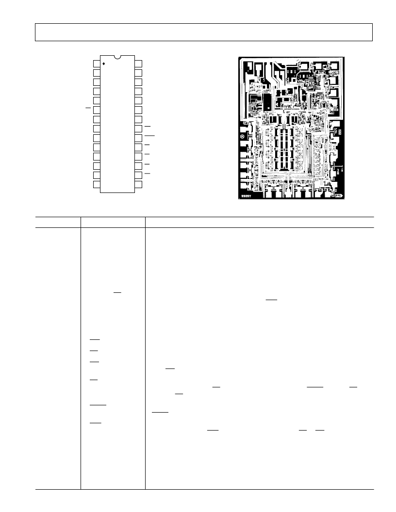
PIN DE SCRIPT IONS
Pin#
Name
Description
1
V
DD
Positive Supply. Nominal value +5 volts. T his pad requires 2 bonds for die assembly.
T he substrate is common with V
DD
.
2
AG
DAC
Analog Ground for the DAC. T here is a separate analog ground for the ADC.
3
V
OUT
Voltage Output from the DAC.
4
NC
No Connect.
5
A1
Address Input that controls multiplexer. See T able I for address decode.
6
RESET (
RS
)
Active Low Digital Input that clears the DAC register to zero, setting the DAC to mini-
mum scale. It also asynchronously clears the
INT
line of the ADC.
7–12, 14, 15
DB7 to DB0
Digital I/O Lines. DB7 (7) is the Most Significant Bit (MSB), for both the ADC and
the DAC, and DB0 (15) is the Least Significant Bit (LSB).
13
DGND
Digital Ground.
16
WR
Rising Edge T riggered Write Input. Used to load data into the DAC register.
17
CS
Chip Select. Active Low Input
18
RD
Active Low Read Input. When this input is active, ADC data can be read from the
part.
RD
going low starts the ADC conversion.
19
ST
Falling Edge T riggered Start Input. Used for applications requiring precise sample tim-
ing. T he falling edge of
ST
starts the conversion and sets the
BUSY
low. T he
ST
is not
gated by
CS
.
20
BUSY
ADC Active Low, Status Output. When the ADC is performing a conversion, the
BUSY
output is low.
21
INT
Active Low Output. T he Interrupt output notifies the system that the ADC has com-
pleted its conversion.
INT
goes high on the rising edge of
CS
or
RD
. It will also be
forced high when RESET is asserted.
22
CLK
External Clock Input Pin. Accepts a T T L or 5 V CMOS input logic levels.
23
AG
ADC
Analog ADC Ground
27–24
V
IN
A, B, C, D
Four Analog Inputs
28
A0
Address input that controls multiplexer. See T able I for address decode.
PIN CONFIGURAT ION
Top View
(Not to Scale)
1
2
3
7
8
9
10
11
12
4
5
6
13
14
28
27
26
22
21
20
19
18
17
25
24
23
16
15
AD8401AR
V
DD
AG
DAC
V
OUT
NC
A1
DB7
DB6
DB5
DB4
DB3
DB2
DGND
DB1
A0
V
IN
A
V
IN
B
V
IN
C
V
IN
D
AG
ADC
CLK
DB0
BUSY
INT
ST
RD
CS
WR
RS
NC = NO CONNECT
DICE CHARACT E RIST ICS
1
2
3
5
6
7
8
9
10
11
12
13
14
15
16
17
18
19
20
21
22
23
24
25
26
27
Die Size 91 X 121 mil = 11,011 sq mil
28
相關PDF資料 |
PDF描述 |
|---|---|
| AD8403 | 4-Channel Digital Potentiometers(???é??é????°?-???μ?????¨) |
| AD841JN | Wideband, Unity-Gain Stable, Fast Settling Op Amp |
| AD841JCHIPS | Wideband, Unity-Gain Stable, Fast Settling Op Amp |
| AD841JH | Wideband, Unity-Gain Stable, Fast Settling Op Amp |
| AD841KH | Wideband, Unity-Gain Stable, Fast Settling Op Amp |
相關代理商/技術參數 |
參數描述 |
|---|---|
| AD8401AR | 制造商:Rochester Electronics LLC 功能描述:8-BIT,4-CHANNEL A/D CONV - Bulk 制造商:Analog Devices 功能描述: |
| AD8401ARZ | 制造商:Analog Devices 功能描述:DATA ACQ SYS SGL ADC SGL DAC 8BIT 28SOIC - Rail/Tube |
| AD8401CHIPS | 制造商:AD 制造商全稱:Analog Devices 功能描述:8-Bit, 4-Channel Data Acquisition System |
| AD8402 | 制造商:AD 制造商全稱:Analog Devices 功能描述:2-Channel, 256-Position Digital Potentiometer |
| AD8402AN1 | 制造商:Rochester Electronics LLC 功能描述:DUAL 8-BIT POTENTIOMETER 1K OHM - Bulk |
發布緊急采購,3分鐘左右您將得到回復。