- 您現在的位置:買賣IC網 > PDF目錄373946 > AD8401 (Analog Devices, Inc.) 8-Bit, 4-Channel Data Acquisition System(8位4通道DAS) PDF資料下載
參數資料
| 型號: | AD8401 |
| 廠商: | Analog Devices, Inc. |
| 英文描述: | 8-Bit, 4-Channel Data Acquisition System(8位4通道DAS) |
| 中文描述: | 8位,4通道數據采集系統(4通道8位DAS)的 |
| 文件頁數: | 6/12頁 |
| 文件大小: | 182K |
| 代理商: | AD8401 |
AD8401
–6–
REV. 0
OPE RAT ION
T he AD8401 is a complete data acquisition and control system.
It contains the DAC, a four channel input multiplexer, a track/
hold, an ADC, as well as an internal bandgap reference. It inter-
faces to the microcontroller via an 8-bit digital I/O port.
D/A CONVE RT E R SE CT ION
T he DAC is an 8-bit voltage mode DAC with an output that
swings from AG
DAC
to the 1.25 volt bandgap voltage. It uses an
R-2R ladder fed by PNP current sources which allow the output
to swing to ground so that the DAC operates in a unipolar mode.
AMPLIFIE R SE CT ION
T he DAC’s output is buffered by an internal high speed op
amp. T he op amps output range is set at 0 V to 2.5 V. T he op
amp has a 500 ns typical settling time to 0.2% for positive
slewing signals. T here are differences in settling time for nega-
tive slewing signals. Signals going to zero volts will settle slightly
slower to ground than is seen in the positive direction.
20
20
V
OUT
V
DD
AG
DAC
n-CH
Figure 3. Equivalent Amplifier Output Stage
Current sinking capability is also limited near zero volts in single
supply operation. Figure 3 provides an equivalent amplifier out-
put stage schematic.
INT E RNAL RE FE RE NCE
An on-chip bandgap is provided as a voltage reference to both
the DAC and the ADC. T his reference is internal to the
AD8401 and is not accessible to the user. It is laser trimmed for
both absolute accuracy and temperature coefficients. T he refer-
ence is internally buffered by a separate control amplifier for both
the DAC and ADC to improve isolation between the converters.
DIGIT AL I/O
T he 8-bit parallel data I/O port on the AD8401 provides access
to both the DAC and the ADC. T his port is T T L/CMOS com-
patible with three-state outputs that are ESD protected.
T he data format is binary. T his data coding applies to both the
DAC and the ADC. See the applications information section.
ADC SE CT ION
A fast successive approximation ADC is used to attain a conver-
sion time of 2 microseconds. Start of conversion is initiated by
CS
and
RD
. Following a Start command the
BUSY
signal will
become active and another Start command should not be given
until the conversion is complete.
T he RESET (
RS
) input does not affect A/D conversion, but the
INT
(Interrupt or conversion complete) which normally goes
active low at the end of a conversion will be forced high by
RESET asynchronously.
Figure 4 shows the wave forms for a conversion cycle. T he track
and hold begins holding the input voltage V
IN
approximately
50 ns after the falling edge of the Start command. T he MSB de-
cision is made approximately 50 ns after the second falling edge
of the CLK . If t
X
is greater than 50 ns, then the falling edge of
the CLK will be seen as the first falling clock edge. If t
X
is less
than 50 ns, the first MSB conversion will not occur until one
clock cycle later. T he following bits will each be converted in a
similar manner 50 ns after each CLK edge until all eight bits
have been converted. After the end of conversion the contents of
the ADC SAR register are transferred to the output data latch,
the track and hold is returned to the track mode,
INT
goes low
and the SAR is reset.
V
IN
CLK
BUSY
CS , RD
OR ST
100ns
TYP
50ns TYP
MSB DECISION
DB7
LSB DECISION
DB0
t
x
50ns TYP
Figure 4. Operating Waveforms Using the External Clock
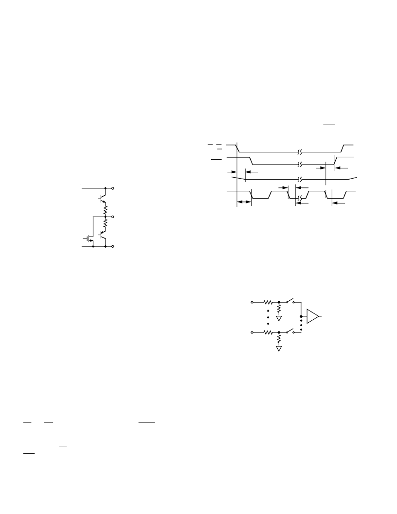
ANALOG INPUT
T he analog inputs of the AD8401 are fed into resistor voltage
divider networks with a typical value of 8.5 k
. T he amplifiers
driving these inputs must have an output resistance low enough
to drive these nodes without losing accuracy. T aps from the
voltage dividers are connected to the track and hold amplifier by
the multiplexer switches.
T/H
V
IN
D
V
IN
A
5k
MUX
AGADC
5k
3.57k
3.57k
Figure 5. Equivalent Analog Input Circuit
T RACK -AND-HOLD AMPLIFIE R
Following the resistive divider at the input of the AD8401 is a
track-and-hold amplifier that captures input signals accurately
up to the 200 kHz Nyquist frequency of the ADC. T o attain this
performance the T /H amplifier must have a much greater band-
width than the signal of interest. Because of this the user must
be careful to band limit the input signal to avoid aliasing high
frequency components and noise into the passband.
T he track-and-hold amplifier is internally controlled by the Start
command and is not directly available to the user. After the
Start command signal the track-and-hold is placed into the hold
mode; it returns to the track mode after the conversion is
complete.
相關PDF資料 |
PDF描述 |
|---|---|
| AD8403 | 4-Channel Digital Potentiometers(???é??é????°?-???μ?????¨) |
| AD841JN | Wideband, Unity-Gain Stable, Fast Settling Op Amp |
| AD841JCHIPS | Wideband, Unity-Gain Stable, Fast Settling Op Amp |
| AD841JH | Wideband, Unity-Gain Stable, Fast Settling Op Amp |
| AD841KH | Wideband, Unity-Gain Stable, Fast Settling Op Amp |
相關代理商/技術參數 |
參數描述 |
|---|---|
| AD8401AR | 制造商:Rochester Electronics LLC 功能描述:8-BIT,4-CHANNEL A/D CONV - Bulk 制造商:Analog Devices 功能描述: |
| AD8401ARZ | 制造商:Analog Devices 功能描述:DATA ACQ SYS SGL ADC SGL DAC 8BIT 28SOIC - Rail/Tube |
| AD8401CHIPS | 制造商:AD 制造商全稱:Analog Devices 功能描述:8-Bit, 4-Channel Data Acquisition System |
| AD8402 | 制造商:AD 制造商全稱:Analog Devices 功能描述:2-Channel, 256-Position Digital Potentiometer |
| AD8402AN1 | 制造商:Rochester Electronics LLC 功能描述:DUAL 8-BIT POTENTIOMETER 1K OHM - Bulk |
發布緊急采購,3分鐘左右您將得到回復。