- 您現在的位置:買賣IC網 > PDF目錄373946 > AD8401 (Analog Devices, Inc.) 8-Bit, 4-Channel Data Acquisition System(8位4通道DAS) PDF資料下載
參數資料
| 型號: | AD8401 |
| 廠商: | Analog Devices, Inc. |
| 英文描述: | 8-Bit, 4-Channel Data Acquisition System(8位4通道DAS) |
| 中文描述: | 8位,4通道數據采集系統(4通道8位DAS)的 |
| 文件頁數: | 7/12頁 |
| 文件大小: | 182K |
| 代理商: | AD8401 |
AD8401
–7–
REV. 0
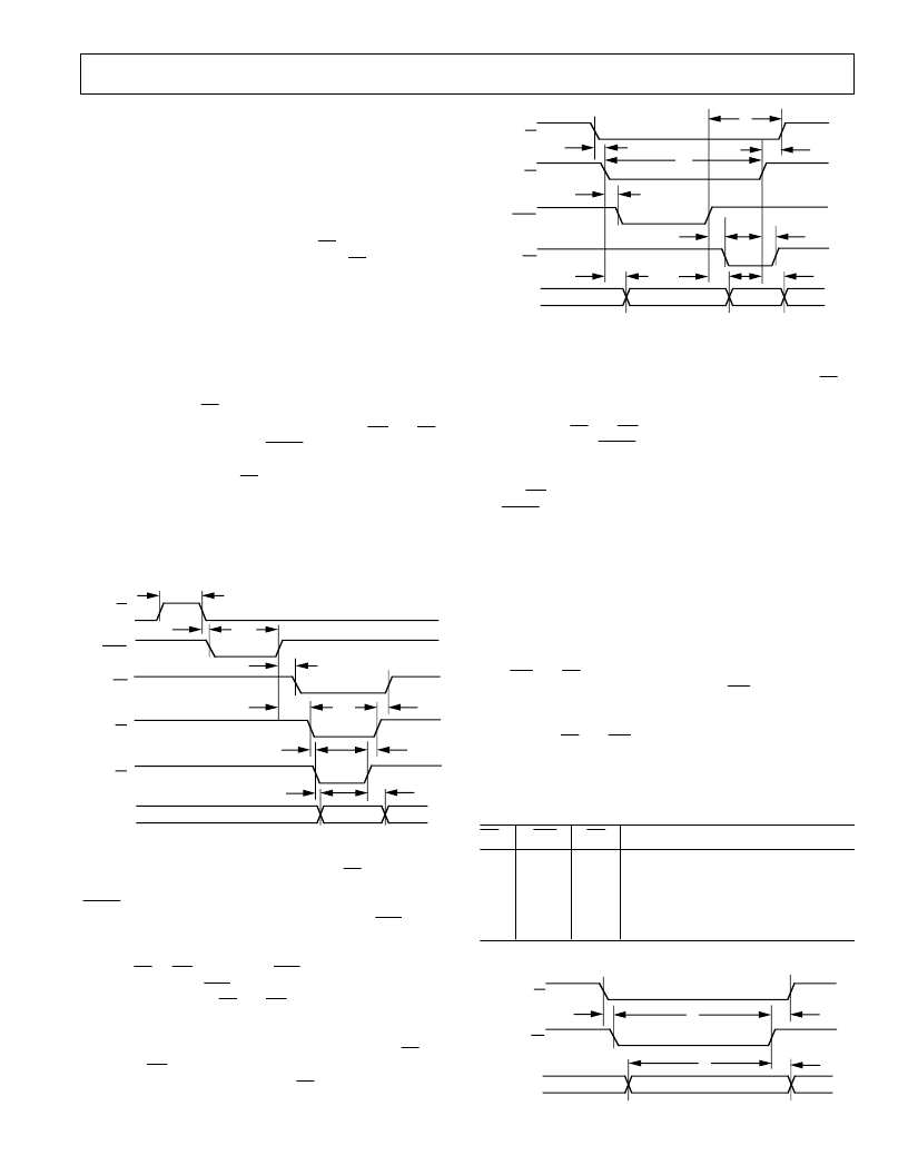
BUSY
t
10
INT
t
16
t
15
CS
t
14
t
8
t
17
RD
DATA
NEW DATA
HIGH Z
OLD DATA
t
12
t
11
t
9
t
13
Figure 7. Mode 2, ADC Interface Timing
Mode 2 Interface
T his interface mode can be used with microprocessors that can
be put into a WAIT state for at least 2 microseconds. T he
ST
pin must be tied to logic high for proper operation. T he micro-
processor begins a conversion by executing a READ instruction
that asserts the
CS
and
RD
pins at the AD8401’s decoded ad-
dress. T he AD8401
BUSY
output then goes low, forcing the
microprocessor’s READY (or WAIT ) line into a WAIT state.
T he analog input signal is captured by the T /H on the falling
edge of
RD
. When the conversion is complete (8 clocks later),
the
BUSY
line returns high, and then the
μ
P completes its
READ of the new data now on the digital output port of the
AD8401. Note that while conversion is in progress the ADC
places the results from the last conversion (Old Data) on the
data bus. T he Figure 7 timing diagram details the applicable
timing specification requirements.
DIGIT AL INT E RFACE : DAC T IMING AND CONT ROL
T able II shows the truth table for DAC operation. T he internal
8-bit DAC register contents are loaded from the data bus when
both
WR
and
CS
are asserted. T he DAC register determines the
D/A converter analog-output voltage. T he
WR
input is a posi-
tive edge triggered input that loads the bus data into the DAC
register subject to the data setup and data hold timing require-
ments. When
CS
and
WR
are low, the DAC register contents
will not change with changing data bus values. Figure 8 provides
the detail timing diagram for write cycle operation.
T able II. DAC Register Logic
CS
WR
RS
DAC Function
H
L
L
`
X
H
L
`
L
X
H
H
H
H
L
No Effect
No Effect
DAC Register Updated
DAC Register Updated
DAC Register Loaded with all Zeros
t
2
CS
t
5
WR
DATA
VALID DATA
t
3
t
1
t
4
Figure 8. Write Cycle Timing
CLOCK
T he AD8401 uses an external clock that is T T L or 5 V CMOS
compatible. T he external clock speed is 5 MHz and the duty
cycle may vary from 30% to 70%. T he external clock can be
continuously operated between conversions.
DIGIT AL INT E RFACE : ADC T IMING AND CONT ROL
T wo basic ADC operating modes are available with the
AD8401. T he first mode uses the Start (
ST
) pin to trigger a
synchronized A/D conversion. As soon as the
ST
pin is asserted,
the T /H switches from tracking to the hold mode capturing the
present analog input-voltage sample. With the T /H holding the
analog sample the successive-approximation analog-to-digital
conversion is completed on that sample value. At the end of
conversion the T /H returns to the tracking mode. T his mode of
conversion is ideal for digital signal processing applications
where precise interval sampling is necessary to minimize errors
due to sampling uncertainty or jitter. A precise clock source can
be used to drive the
ST
input.
T he second mode of conversion is started by the
RD
and
CS
in-
puts going low, after which the
BUSY
line puts the micropro-
cessor into a WAIT state until end of conversion. Mode 2 is
asserted by connecting the
ST
pin to logic high. T he major ad-
vantage of this interface is that a single Read Instruction will
start and complete a new analog-to-digital conversion without
the need for carefully tailored software delays that often are not
portable when software routines are taken to a different proces-
sor running at a different clock speed.
BUSY
ST
t
6
t
7
t
CONVERT
t
8
INT
t
9
t
15
t
12
CS
t
14
t
11
t
10
t
13
RD
DATA
DATA VALID
HIGH Z
Figure 6. Mode 1, ADC Interface Timing
Mode 1 Interface
As shown in Figure 6, the falling edge of the
ST
pulse initiates a
conversion and puts the T /H amplifier into the hold mode. T he
BUSY
signal goes low during the whole A/D conversion time
and returns high signaling end of conversion. T he
INT
line can
be used to interrupt the microprocessor. When the microproces-
sor performs a READ to access the AD8401 data, the rising
edges of
CS
or
RD
will reset the
INT
output to high after the t
15
timing specification.
INT
can also be used to externally trigger a
pulse that activates the
CS
and
RD
and places the new data into
a buffer or First In First Out FIFO memory. T he microproces-
sor can then load a series of readings from this buffer memory at
a convenient time. Care must be taken not to have the
ST
input
high when
RD
is brought low; otherwise, the AD8401 will not
operate properly. Also triggering the
ST
line a second time be-
fore conversion is complete will cause erroneous readings.
相關PDF資料 |
PDF描述 |
|---|---|
| AD8403 | 4-Channel Digital Potentiometers(???é??é????°?-???μ?????¨) |
| AD841JN | Wideband, Unity-Gain Stable, Fast Settling Op Amp |
| AD841JCHIPS | Wideband, Unity-Gain Stable, Fast Settling Op Amp |
| AD841JH | Wideband, Unity-Gain Stable, Fast Settling Op Amp |
| AD841KH | Wideband, Unity-Gain Stable, Fast Settling Op Amp |
相關代理商/技術參數 |
參數描述 |
|---|---|
| AD8401AR | 制造商:Rochester Electronics LLC 功能描述:8-BIT,4-CHANNEL A/D CONV - Bulk 制造商:Analog Devices 功能描述: |
| AD8401ARZ | 制造商:Analog Devices 功能描述:DATA ACQ SYS SGL ADC SGL DAC 8BIT 28SOIC - Rail/Tube |
| AD8401CHIPS | 制造商:AD 制造商全稱:Analog Devices 功能描述:8-Bit, 4-Channel Data Acquisition System |
| AD8402 | 制造商:AD 制造商全稱:Analog Devices 功能描述:2-Channel, 256-Position Digital Potentiometer |
| AD8402AN1 | 制造商:Rochester Electronics LLC 功能描述:DUAL 8-BIT POTENTIOMETER 1K OHM - Bulk |
發布緊急采購,3分鐘左右您將得到回復。