- 您現在的位置:買賣IC網 > PDF目錄373949 > AD8555 (Analog Devices, Inc.) Zero-Drift, Digitally Programmable Sensor Signal Amplifier PDF資料下載
參數資料
| 型號: | AD8555 |
| 廠商: | Analog Devices, Inc. |
| 英文描述: | Zero-Drift, Digitally Programmable Sensor Signal Amplifier |
| 中文描述: | 零漂移,數字可編程傳感器信號放大器 |
| 文件頁數: | 1/28頁 |
| 文件大小: | 503K |
| 代理商: | AD8555 |
當前第1頁第2頁第3頁第4頁第5頁第6頁第7頁第8頁第9頁第10頁第11頁第12頁第13頁第14頁第15頁第16頁第17頁第18頁第19頁第20頁第21頁第22頁第23頁第24頁第25頁第26頁第27頁第28頁
Zero-Drift, Digitally Programmable
Sensor Signal Amplifier
AD8555
FEATURES
Rev.
0
Information furnished by Analog Devices is believed to be accurate and reliable.
However, no responsibility is assumed by Analog Devices for its use, nor for any
infringements of patents or other rights of third parties that may result from its use.
Specifications subject to change without notice. No license is granted by implication
or otherwise under any patent or patent rights of Analog Devices. Trademarks and
registered trademarks are the property of their respective owners.
Tel: 781.329.4700Fax: 781.326.8703
Very low offset voltage: 10 μV maximum over temperature Very low input offset voltage drift: 60 nV/°C maximum
High CMRR: 96 dB minimum
Digitally programmable gain and output offset voltage
Single-wire serial interface
Open and short wire fault detection
Low-pass filtering
Stable with any capacitive load
Externally programmable output clamp voltage for driving
low voltage ADCs
LFCSP-16 and SOIC-8 packages
2.7 V to 5.5 V operation
40°C to +125°C operation
APPLICATIONS
Automotive sensors
Pressure and position sensors
Thermocouple amplifiers
Industrial weigh scales
Precision current sensing
Strain gages
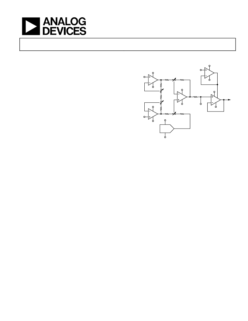
FUNCTIONAL BLOCK DIAGRAM
A3
A2
A4
A5
VDD
VDD
DAC
VSS
VSS
VDD
VSS
VDD
VDD
VSS
VCLAMP
VPOS
VSS
FILT/
DIGOUT
VOUT
A1
VDD
VSS
VNEG
R1
R3
R2
R5
R7
P4
R4
R6
RF
P3
P2
P1
0
Figure 1.
GENERAL DESCRIPTION
The AD8555 is a zero-drift, sensor signal amplifier with digi-
tally programmable gain and output offset. Designed to easily
and accurately convert variable pressure sensor and strain
bridge outputs to a well-defined output voltage range, the
AD8555 also accurately amplifies many other differential or
single-ended sensor outputs. The AD8555 uses the ADI pat-
ented low noise auto-zero and DigiTrim technologies to create
an incredibly accurate and flexible signal processing solution in
a very compact footprint.
Gain is digitally programmable in a wide range from 70 to 1,280
through a serial data interface. Gain adjustment can be fully
simulated in-circuit and then permanently programmed with
proven and reliable poly-fuse technology. Output offset voltage
is also digitally programmable and is ratiometric to the supply
voltage.
In addition to extremely low input offset voltage and input off-
set voltage drift and very high dc and ac CMRR, the AD8555
also includes a pull-up current source at the input pins and a
pull-down current source at the VCLAMP pin. This allows open
wire and shorted wire fault detection. A low-pass filter function
is implemented via a single low cost external capacitor. Output
clamping set via an external reference voltage allows the
AD8555 to drive lower voltage ADCs safely and accurately.
When used in conjunction with an ADC referenced to the same
supply, the system accuracy becomes immune to normal supply
voltage variations. Output offset voltage can be adjusted with a
resolution of better than 0.4% of the difference between VDD
and VSS. A lockout trim after gain and offset adjustment further
ensures field reliability.
The AD8555AR is fully specified over the extended industrial
temperature range of 40°C to +125°C. Operating from
single-supply voltages of 2.7 V to 5.5 V, the AD8555 is offered in
the narrow 8-lead SOIC package and the 4 mm × 4 mm
16-lead LFCSP.
相關PDF資料 |
PDF描述 |
|---|---|
| AD8555ACP-R2 | Zero-Drift, Digitally Programmable Sensor Signal Amplifier |
| AD8555ACP-REEL | Zero-Drift, Digitally Programmable Sensor Signal Amplifier |
| AD8561AR | Ultrafast 7 ns Single Supply Comparator |
| AD8561ARU | Ultrafast 7 ns Single Supply Comparator |
| AD8561AN | Ultrafast 7 ns Single Supply Comparator |
相關代理商/技術參數 |
參數描述 |
|---|---|
| AD8555_09 | 制造商:AD 制造商全稱:Analog Devices 功能描述:Zero-Drift, Digitally Programmable Sensor Signal Amplifier |
| AD85551 | 制造商:AD 制造商全稱:Analog Devices 功能描述:10 MHz, 20 V/レs, G = 1, 10, 100, 1000 i CMOS㈢ Programmable Gain Instrumentation Amplifier |
| AD8555ACP | 制造商:Analog Devices 功能描述:SP AMP CURRENT SENSE AMP SGL R-R I/O 5.5V 16LFCSP EP - Bulk |
| AD8555ACP-R2 | 制造商:Analog Devices 功能描述:SP Amp Current Sense Amp Single R-R I/O 5.5V 16-Pin LFCSP EP T/R 制造商:Rochester Electronics LLC 功能描述:AUTO ZERO AMP W/PROGRAMMABLE GAIN/OFFSET - Bulk |
| AD8555ACP-REEL | 制造商:Analog Devices 功能描述:SP Amp Current Sense Amp Single R-R I/O 5.5V 16-Pin LFCSP EP T/R |
發布緊急采購,3分鐘左右您將得到回復。