- 您現(xiàn)在的位置:買賣IC網(wǎng) > PDF目錄373949 > AD8555AR (ANALOG DEVICES INC) Zero-Drift, Digitally Programmable Sensor Signal Amplifier PDF資料下載
參數(shù)資料
| 型號: | AD8555AR |
| 廠商: | ANALOG DEVICES INC |
| 元件分類: | 模擬信號調(diào)理 |
| 英文描述: | Zero-Drift, Digitally Programmable Sensor Signal Amplifier |
| 中文描述: | SPECIALTY ANALOG CIRCUIT, PDSO8 |
| 封裝: | MS-012AA, SOIC-8 |
| 文件頁數(shù): | 26/28頁 |
| 文件大小: | 503K |
| 代理商: | AD8555AR |
第1頁第2頁第3頁第4頁第5頁第6頁第7頁第8頁第9頁第10頁第11頁第12頁第13頁第14頁第15頁第16頁第17頁第18頁第19頁第20頁第21頁第22頁第23頁第24頁第25頁當(dāng)前第26頁第27頁第28頁
AD8555
Rev. 0 | Page 26 of 28
0
LOAD CAPACITANCE (nF)
100.0
0.1
1.0
10.0
O
60
50
40
30
20
10
0
R
S
C
L
V
S
= ±2.5V
R
S
= 0
R
S
= 10
R
S
= 20
R
S
= 50
R
S
= 100
Figure 58. Negative Overshoot Graph vs. C
L
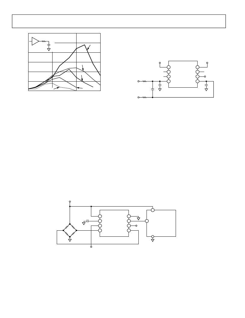
RF INTERFERENCE
All instrumentation amplifiers show dc offset as the result of
rectification of high frequency out-of-band signals that appear
at their inputs. The circuit in Figure 59 provides good RFI sup-
pression without reducing performance within the AD8555 pass
band. Resistor R1 and Capacitor C1, and likewise Resistor R2
and Capacitor C2, form a low-pass RC filter that has a 3 dB
bandwidth equal to f
(3 dB)
= 1/2 π × R1 × C1. It can be seen that
R1, R2 and C1, C2 form a bridge circuit whose output appears
across the amplifier’s input pins. Any mismatch between C1, C2
unbalances the bridge and reduce the common-mode rejection.
Using the component values shown, this filter has a bandwidth
of approximately 40 kHz. To preserve common-mode rejection
in the AD8555’s pass band, capacitors need to be 5% (silver
mica) or better and should be placed as close to its inputs as
possible. Resistors should be 1% metal film. Capacitor C3 is
needed to maintain common-mode rejection at low frequencies.
This introduces a second low-pass network, R1 + R2 and C3
that has a 3 dB frequency equal to 1/(2 π × (R1 + R2)(C3)).
This circuit’s 3 dB signal bandwidth is approximately 4 kHz
when a C3 value of 0.047 μF is used (see Figure 59).
1
2
3
4
5
6
7
8
AD8555
VDD
FILT/DIGOUT
DIGIN
VNEG
VSS
VOUT
VCLAMP
VPOS
VPOS
VDD
VDD
VSS
0
VNEG
R2
4.02k
R1
4.02k
C3
0.047
μ
F
C2
1nF
C1
1nF
Figure 59. RFI Suppression Method
SINGLE-SUPPLY DATA ACQUISITION SYSTEM
Interfacing bipolar signals to single-supply analog-to-digital
converters (ADCs) presents a challenge. The bipolar signal must
be mapped into the input range of the ADC. Figure 60 shows
how this translation can be achieved. The output offset can be
programmed to a desirable level to accommodate the input
voltage requirement of the ADC.
1
2
3
4
5
6
7
8
AD8555
VDD
FILT/DIGOUT
DIGIN
VNEG
2
4
AD7476
12 BIT
AIN
V
DD
VSS
VOUT
VCLAMP
VPOS
VDD
0
VDD
S
DIGIN
10nF
0
100
100
100
100
Figure 60. A Single-Supply Data Acquisition Circuit Using the AD8555
相關(guān)PDF資料 |
PDF描述 |
|---|---|
| AD8555AR-REEL7 | Zero-Drift, Digitally Programmable Sensor Signal Amplifier |
| AD8555 | Zero-Drift, Digitally Programmable Sensor Signal Amplifier |
| AD8555ACP-R2 | Zero-Drift, Digitally Programmable Sensor Signal Amplifier |
| AD8555ACP-REEL | Zero-Drift, Digitally Programmable Sensor Signal Amplifier |
| AD8561AR | Ultrafast 7 ns Single Supply Comparator |
相關(guān)代理商/技術(shù)參數(shù) |
參數(shù)描述 |
|---|---|
| AD8555AR-EVAL | 制造商:Analog Devices 功能描述:Evaluation Board For Zero-Drift, Digitally Programmable Sensor Signal Amplifier |
| AD8555AR-REEL | 制造商:Analog Devices 功能描述:SP Amp Current Sense Amp Single R-R I/O 5.5V 8-Pin SOIC N T/R |
| AD8555AR-REEL7 | 制造商:Analog Devices 功能描述:SP Amp Current Sense Amp Single R-R I/O 5.5V 8-Pin SOIC N T/R |
| AD8555ARZ | 功能描述:IC AMP CHOPPER 2MHZ 10MA 8SOIC RoHS:是 類別:集成電路 (IC) >> Linear - Amplifiers - Instrumentation 系列:DigiTrim® 標(biāo)準(zhǔn)包裝:2,500 系列:- 放大器類型:通用 電路數(shù):4 輸出類型:- 轉(zhuǎn)換速率:0.6 V/µs 增益帶寬積:1MHz -3db帶寬:- 電流 - 輸入偏壓:45nA 電壓 - 輸入偏移:2000µV 電流 - 電源:1.4mA 電流 - 輸出 / 通道:40mA 電壓 - 電源,單路/雙路(±):3 V ~ 32 V,±1.5 V ~ 16 V 工作溫度:0°C ~ 70°C 安裝類型:表面貼裝 封裝/外殼:14-TSSOP(0.173",4.40mm 寬) 供應(yīng)商設(shè)備封裝:14-TSSOP 包裝:帶卷 (TR) 其它名稱:LM324ADTBR2G-NDLM324ADTBR2GOSTR |
| AD8555ARZ1 | 制造商:AD 制造商全稱:Analog Devices 功能描述:Zero-Drift, Digitally Programmable Sensor Signal Amplifier |
發(fā)布緊急采購,3分鐘左右您將得到回復(fù)。