- 您現在的位置:買賣IC網 > PDF目錄373959 > AD9203-EB (Analog Devices, Inc.) 10-Bit, 40 MSPS, 3 V, 74 mW A/D Converter PDF資料下載
參數資料
| 型號: | AD9203-EB |
| 廠商: | Analog Devices, Inc. |
| 英文描述: | 10-Bit, 40 MSPS, 3 V, 74 mW A/D Converter |
| 中文描述: | 10位,40 MSPS的,3伏,74毫瓦的A / D轉換器 |
| 文件頁數: | 14/19頁 |
| 文件大小: | 216K |
| 代理商: | AD9203-EB |

REV. 0
AD9203
–14–
POWER CONTROL
Power consumed by the AD9203 may be reduced by placing a
resistor between the PWRCON pin and ground. This function
will be valuable to users who do not need the AD9203’s high
conversion rate, but do need even lower power consumption.
The external resistor sets the programming of the analog current
mirrors. Table II illustrates the relationship between programmed
power and performance.
At lower clock rates, less power is required within the analog
sections of the AD9203. Placing an external resistor on the
PWRCON pin will shunt control current away from some of the
current mirrors. This enables the ADC to convert low data rates
with extremely low power consumption.
INTERFACING TO 5 V SYSTEMS
The AD9203 can be integrated into +5 V systems. This is
accomplished by deriving a 3 V power supply from the existing
5 V analog power line through an AD3307-3 linear regulator.
Care must be maintained so that logic inputs do not exceed the
maximum rated values listed on the Specifications page.
CLOCK INPUT AND CONSIDERATIONS
The AD9203 internal timing uses the two edges of the clock
input to generate a variety of internal timing signals. Sampling
occurs on the falling edge. The clock input to the AD9203
operating at 40 MSPS may have a duty cycle between 45% to
55% to meet this timing requirement since the minimum speci-
fied t
CH
and t
CL
is 11.25 ns. For clock rates below 40 MSPS, the
duty cycle may deviate from this range to the extent that both
t
CH
and t
CL
are satisfied. See Figure 29 for dynamics vs. duty
cyle.
High speed high resolution A/Ds are sensitive to the quality of
the clock input. The degradation in SNR at a given full-scale
input frequency (f
IN
) due only to aperture jitter (t
A
) can be
calculated with the following equation:
SNR degradation
= 20 log
10
[1/2
π
f
IN
t
A
]
In the equation, the rms aperture jitter,
t
A
, represents the root-
sum square of all the jitter sources, which include the clock in-
put, analog input signal, and A/D aperture jitter specification.
Undersampling applications are particularly sensitive to jitter.
Clock input should be treated as an analog signal in cases where
aperture jitter may affect the dynamic range of the AD9203.
Power supplies for clock drivers should be separated from the
A/D output driver supplies to avoid modulating the clock signal
with digital noise. Low jitter crystal controlled oscillators make
the best clock sources. If the clock is generated from another
type of source (by gating, dividing or other method), it should
be retimed by the original clock at the last step.
The clock input is referred to the analog supply. Its logic thresh-
old is AVDD/2.
DIGITAL INPUTS AND OUTPUTS
Each of the AD9203 digital control inputs, 3-STATE, DFS and
STBY are referenced to analog ground. CLK is also referenced
to analog ground. A low power mode feature is provided such
that for STBY = HIGH and the static power of the AD9203 drops
to 0.65 mW.
Asserting the DFS pin high will invert the MSB pin, changing
the data to a twos complement format.
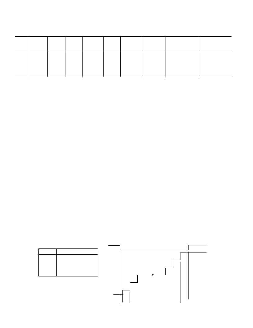
The AD9203 has an OTR (out of range) function. If the input
voltage is above or below full scale by 1 LSB, the OTR flag will
go high. See Figure 30.
+FS
–FS
OTR
DATA OUTPUTS
1
0
0
11111
11111
11111
11111
11111
11110
0
0
1
00000
00000
00000
00001
00000
00000
OTR
+FS – 1 LSB
–FS + 1 LSB
Figure 30. Output Data Format
Table II. Power Programming Resistance
Total Power
Into 5 pF Load
mW
Power Control
Resistor
k
V
Clock
MHz
f
IN
MHz
THD
dB
SNR
dB
SINAD
dB
SFDR
dB
IAVDD
mA
IDRVDD
mA
5
10
15
20
30
2.5
2.5
2.5
5
5
–72
–74.3
–74
–75.1
–75
60.6
60.7
60.1
53.4
59.5
59.9
60.4
59.9
53.2
59.4
77.9
77.8
77.7
78.9
74.8
5.0
5.9
6.7
7.8
10
0.86
1.2
1.8
2.4
4.0
17
21.3
25
30
42
37
37
37
50
50
相關PDF資料 |
PDF描述 |
|---|---|
| AD9203ARU | 10-Bit, 40 MSPS, 3 V, 74 mW A/D Converter |
| AD9211_07 | 10-Bit, 200 MSPS/250 MSPS/300 MSPS, 1.8 V Analog-to-Digital Converter |
| AD9211-200EBZ | 10-Bit, 200 MSPS/250 MSPS/300 MSPS, 1.8 V Analog-to-Digital Converter |
| AD9211-250EBZ | 10-Bit, 200 MSPS/250 MSPS/300 MSPS, 1.8 V Analog-to-Digital Converter |
| AD9211-300EBZ | 10-Bit, 200 MSPS/250 MSPS/300 MSPS, 1.8 V Analog-to-Digital Converter |
相關代理商/技術參數 |
參數描述 |
|---|---|
| AD9203-EBZ | 制造商:Analog Devices 功能描述:EVAL KIT FOR 10-BIT, 40 MSPS, 3V, 74 MW A/D CNVRTR - Bulk |
| AD9203W | 制造商:AD 制造商全稱:Analog Devices 功能描述:10-Bit, 40 MSPS, 3 V, 74 mW Analog-to-Digital Converter |
| AD9203WARUZ | 制造商:Analog Devices 功能描述: |
| AD9203WARUZRL7 | 制造商:AD 制造商全稱:Analog Devices 功能描述:10-Bit, 40 MSPS, 3 V, 74 mW Analog-to-Digital Converter |
| AD9204-20EBZ | 功能描述:BOARD EVALUATION 20MSPS AD9204 RoHS:是 類別:編程器,開發系統 >> 評估板 - 模數轉換器 (ADC) 系列:- 產品培訓模塊:Obsolescence Mitigation Program 標準包裝:1 系列:- ADC 的數量:1 位數:12 采樣率(每秒):94.4k 數據接口:USB 輸入范圍:±VREF/2 在以下條件下的電源(標準):- 工作溫度:-40°C ~ 85°C 已用 IC / 零件:MAX11645 已供物品:板,軟件 |
發布緊急采購,3分鐘左右您將得到回復。