- 您現(xiàn)在的位置:買賣IC網(wǎng) > PDF目錄373959 > AD9203-EB (Analog Devices, Inc.) 10-Bit, 40 MSPS, 3 V, 74 mW A/D Converter PDF資料下載
參數(shù)資料
| 型號: | AD9203-EB |
| 廠商: | Analog Devices, Inc. |
| 英文描述: | 10-Bit, 40 MSPS, 3 V, 74 mW A/D Converter |
| 中文描述: | 10位,40 MSPS的,3伏,74毫瓦的A / D轉(zhuǎn)換器 |
| 文件頁數(shù): | 9/19頁 |
| 文件大小: | 216K |
| 代理商: | AD9203-EB |
REV. 0
AD9203
–9–
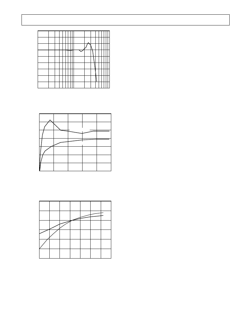
INPUT FREQUENCY – MHz
0
–1
10
1000
100
A
–2
–3
–4
–5
–6
–7
–8
–9
Figure 14. Full Power Bandwidth
OFF-TIME – ms
3500
0
W
m
s
3000
2500
2000
1500
500
0
200
400
600
800
1000
1000
0.5V REFERENCE
1V REFERENCE
Figure 15. Wake-Up Time vs. Off Time (VREF Decoupling
= 10
μ
F)
TEMPERATURE –
8
C
0.2
–40
V
R
0.1
0
–0.1
–0.2
–0.3
–0.4
–20
0
20
40
60
80
100
1V
0.5V
Figure 16. Reference Voltage vs. Temperature
APPLYING THE AD9203
THEORY OF OPERATION
The AD9203 implements a pipelined multistage architecture to
achieve high sample rates while consuming low power. The
AD9203 distributes the conversion over several smaller A/D
subblocks, refining the conversion with progressively higher
accuracy as it passes the results from stage to stage. As a conse-
quence of the distributed conversion, the AD9203 requires a
small fraction of the 1023 comparators used in a traditional
10-bit flash-type A/D. A sample-and-hold function within each
of the stages permits the first stage to operate on a new input
sample while the remaining stages operate on preceding samples.
Each stage of the pipeline, excluding the last, consists of a low
resolution flash A/D connected to a switched capacitor DAC
and interstage residue amplifier (MDAC). The residue amplifier
magnifies the difference between the reconstructed DAC output
and the flash input for the next stage in the pipeline. One bit of
redundancy is used in each one of the stages to facilitate digital
correction of flash errors. The last stage simply consists of a
flash A/D.
The input of the AD9203 incorporates a novel structure that
merges the input sample and hold amplifier (SHA) and the first
pipeline residue amplifier into a single, compact switched ca-
pacitor circuit. This structure achieves considerable noise and
power savings over a conventional implementation that uses
separate amplifiers by eliminating one amplifier in the pipeline.
By matching the sampling network of the input SHA with the
first stage flash A/D, the AD9203 can sample inputs well beyond
the Nyquist frequency with no degradation in performance.
Sampling occurs on the falling edge of the clock.
OPERATIONAL MODES
The AD9203 may be connected in several input configurations
(see Table I).
The AD9203 may be driven differentially from a source that
keeps the signal peaks within the power supply rails.
Alternatively, the input may be driven into AINP or AINN from
a single-ended source. The input span will be 2
×
the programmed
reference voltage. One input will accept the signal, while the
opposite input will be set to midscale by connecting it to the
internal or an external reference. For example, a 2 V p-p signal
may be applied to AINP while a 1 V reference is applied to AINN.
The AD9203 will then accept a signal varying between 2 V and
0 V. See Figures 17, 18 and 19 for more details.
The AD9203’s single-ended (ac-coupled) input may also be
clamped to ground by the AD9203’s internal clamp switch. This
is accomplished by connecting the CLAMP pin to AINN or AINP.
Digital output formats may be configured in binary and twos
complement. This is determined by the potential on the DFS
pin. If the pin is set to Logic “0,” the data will be in straight
binary format. If the pin is asserted to Logic “1,” the data will be in
twos complement format.
Power consumption may be reduced by placing a resistor be-
tween PWRCON and AVSS. This may be done to conserve
power when not encoding high speed analog input frequencies
or sampling at the maximum conversion rate. See Power Con-
trol section.
相關(guān)PDF資料 |
PDF描述 |
|---|---|
| AD9203ARU | 10-Bit, 40 MSPS, 3 V, 74 mW A/D Converter |
| AD9211_07 | 10-Bit, 200 MSPS/250 MSPS/300 MSPS, 1.8 V Analog-to-Digital Converter |
| AD9211-200EBZ | 10-Bit, 200 MSPS/250 MSPS/300 MSPS, 1.8 V Analog-to-Digital Converter |
| AD9211-250EBZ | 10-Bit, 200 MSPS/250 MSPS/300 MSPS, 1.8 V Analog-to-Digital Converter |
| AD9211-300EBZ | 10-Bit, 200 MSPS/250 MSPS/300 MSPS, 1.8 V Analog-to-Digital Converter |
相關(guān)代理商/技術(shù)參數(shù) |
參數(shù)描述 |
|---|---|
| AD9203-EBZ | 制造商:Analog Devices 功能描述:EVAL KIT FOR 10-BIT, 40 MSPS, 3V, 74 MW A/D CNVRTR - Bulk |
| AD9203W | 制造商:AD 制造商全稱:Analog Devices 功能描述:10-Bit, 40 MSPS, 3 V, 74 mW Analog-to-Digital Converter |
| AD9203WARUZ | 制造商:Analog Devices 功能描述: |
| AD9203WARUZRL7 | 制造商:AD 制造商全稱:Analog Devices 功能描述:10-Bit, 40 MSPS, 3 V, 74 mW Analog-to-Digital Converter |
| AD9204-20EBZ | 功能描述:BOARD EVALUATION 20MSPS AD9204 RoHS:是 類別:編程器,開發(fā)系統(tǒng) >> 評估板 - 模數(shù)轉(zhuǎn)換器 (ADC) 系列:- 產(chǎn)品培訓(xùn)模塊:Obsolescence Mitigation Program 標(biāo)準(zhǔn)包裝:1 系列:- ADC 的數(shù)量:1 位數(shù):12 采樣率(每秒):94.4k 數(shù)據(jù)接口:USB 輸入范圍:±VREF/2 在以下條件下的電源(標(biāo)準(zhǔn)):- 工作溫度:-40°C ~ 85°C 已用 IC / 零件:MAX11645 已供物品:板,軟件 |
發(fā)布緊急采購,3分鐘左右您將得到回復(fù)。